As a third-generation semiconductor substrate material, silicon carbide (SiC) single crystal has broad application prospects in the manufacturing of high-frequency and high-power electronic devices. The processing technology of SiC plays a decisive role in the production of high-quality substrate materials. This article introduces the current state of research on SiC processing technologies both in China and abroad, analyzing and comparing the mechanisms of cutting, grinding, and polishing processes, as well as the trends in wafer flatness and surface roughness. It also points out the existing challenges in SiC wafer processing and discusses future development directions.
Silicon carbide (SiC) wafers are critical foundational materials for third-generation semiconductor devices and hold significant importance and market potential in fields such as microelectronics, power electronics, and semiconductor lighting. Due to the extremely high hardness and chemical stability of SiC single crystals, traditional semiconductor processing methods are not entirely suitable for their machining. Although many international companies have conducted extensive research on the technically demanding processing of SiC single crystals, relevant technologies are kept strictly confidential.
In recent years, China has increased efforts in the development of SiC single crystal materials and devices. However, the advancement of SiC device technology in the country is currently constrained by limitations in processing technologies and wafer quality. Therefore, it is essential for China to improve SiC processing capabilities to enhance the quality of SiC single crystal substrates and achieve their practical application and mass production.
The main processing steps include: cutting → coarse grinding → fine grinding → rough polishing (mechanical polishing) → fine polishing (chemical mechanical polishing, CMP) → inspection.
|
Step |
SiC Wafer Processing |
Traditional Semiconductor Single-Crystal Material Processing |
| Cutting | Uses multi-wire sawing technology to slice SiC ingots into thin wafers | Typically uses inner-diameter or outer-diameter blade cutting techniques |
| Grinding | Divided into coarse and fine grinding to remove saw marks and damage layers caused by cutting | Grinding methods may vary, but the goal is the same |
| Polishing | Includes rough and ultra-precision polishing using mechanical and chemical mechanical polishing (CMP) | Usually includes chemical mechanical polishing (CMP), though specific steps may differ |
Cutting of SiC Single Crystals
In the processing of SiC single crystals, cutting is the first and a highly critical step. The wafer’s bow, warp, and total thickness variation (TTV) resulting from the cutting process determine the quality and effectiveness of subsequent grinding and polishing operations.
Cutting tools can be categorized by shape into diamond inner diameter (ID) saws, outer diameter (OD) saws, band saws, and wire saws. Wire saws, in turn, can be classified by their motion type into reciprocating and loop (endless) wire systems. Based on the cutting mechanism of the abrasive, wire saw slicing techniques can be divided into two types: free abrasive wire sawing and fixed abrasive diamond wire sawing.
1.1 Traditional Cutting Methods
The cutting depth of outer diameter (OD) saws is limited by the diameter of the blade. During the cutting process, the blade is prone to vibration and deviation, resulting in high noise levels and poor rigidity. Inner diameter (ID) saws use diamond abrasives on the inner circumference of the blade as the cutting edge. These blades can be as thin as 0.2 mm. During slicing, the ID blade rotates at high speed while the material to be cut moves radially relative to the blade’s center, achieving slicing through this relative motion.
Diamond band saws require frequent stops and reversals, and the cutting speed is very low—typically not exceeding 2 m/s. They also suffer from significant mechanical wear and high maintenance costs. Due to the width of the saw blade, the cutting radius cannot be too small, and multi-slice cutting is not possible. These traditional sawing tools are limited by the rigidity of the base and cannot make curved cuts or have restricted turning radii. They are only capable of straight cuts, produce wide kerfs, have a low yield rate, and are thus unsuitable for cutting SiC crystals.
1.2 Free Abrasive Wire Saw Multi-Wire Cutting
The free abrasive wire saw slicing technique uses the rapid movement of the wire to carry slurry into the kerf, enabling material removal. It primarily employs a reciprocating structure and is currently a mature and widely used method for efficient multi-wafer cutting of single-crystal silicon. However, its application in SiC cutting has been less extensively studied.
Free abrasive wire saws can process wafers with thicknesses less than 300 μm. They offer low kerf loss, rarely cause chipping, and result in relatively good surface quality. However, due to the material removal mechanism—based on the rolling and indentation of abrasives—the wafer surface tends to develop significant residual stress, microcracks, and deeper damage layers. This leads to wafer warping, makes it difficult to control the surface profile accuracy, and increases the load on subsequent processing steps.
The cutting performance is heavily influenced by the slurry; it is necessary to maintain the sharpness of the abrasives and the concentration of the slurry. Slurry treatment and recycling are costly. When cutting large-sized ingots, abrasives have difficulty penetrating deep and long kerfs. Under the same abrasive grain size, the kerf loss is greater than that of fixed-abrasive wire saws.
1.3 Fixed Abrasive Diamond Wire Saw Multi-Wire Cutting
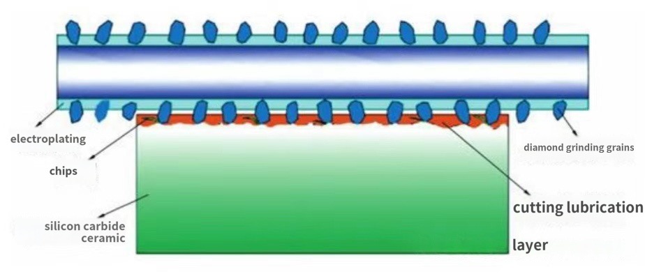
Fixed abrasive diamond wire saws are typically made by embedding diamond particles onto a steel wire substrate through electroplating, sintering, or resin bonding methods. Electroplated diamond wire saws offer advantages such as narrower kerfs, better slice quality, higher efficiency, lower contamination, and the ability to cut high-hardness materials.
The reciprocating electroplated diamond wire saw is currently the most widely used method for cutting SiC. Figure 1 (not shown here) illustrates the surface flatness of SiC wafers cut using this technique. As cutting progresses, wafer warpage increases. This is because the contact area between the wire and the material increases as the wire moves downward, increasing resistance and wire vibration. When the wire reaches the wafer’s maximum diameter, the vibration is at its peak, resulting in maximum warpage.
In the later stages of cutting, due to the wire undergoing acceleration, stable-speed movement, deceleration, stopping, and reversal, along with difficulties in removing debris with the coolant, the surface quality of the wafer deteriorates. Wire reversal and speed fluctuations, as well as large diamond particles on the wire, are the primary causes of surface scratches.
1.4 Cold Separation Technology
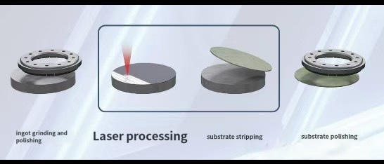
Cold separation of SiC single crystals is an innovative process in the field of third-generation semiconductor material processing. In recent years, it has attracted significant attention due to its notable advantages in improving yield and reducing material loss. The technology can be analyzed from three aspects: working principle, process flow, and core advantages.
Crystal Orientation Determination and Outer Diameter Grinding: Prior to processing, the crystal orientation of the SiC ingot must be determined. The ingot is then shaped into a cylindrical structure (commonly called a SiC puck) via outer diameter grinding. This step lays the foundation for subsequent directional cutting and slicing.
Multi-Wire Cutting: This method uses abrasive particles combined with cutting wires to slice the cylindrical ingot. However, it suffers from significant kerf loss and surface unevenness issues.
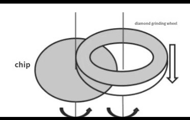
Laser Cutting Technology: A laser is used to form a modified layer within the crystal, from which thin slices can be detached. This approach reduces material loss and enhances processing efficiency, making it a promising new direction for SiC wafer cutting.
Cutting Process Optimization
Fixed Abrasive Multi-Wire Cutting: This is currently the mainstream technology, well-suited for the high hardness characteristics of SiC.
Electrical Discharge Machining (EDM) and Cold Separation Technology: These methods provide diversified solutions tailored to specific requirements.
Polishing Process: It is essential to balance material removal rate and surface damage. Chemical Mechanical Polishing (CMP) is employed to improve surface uniformity.
Real-Time Monitoring: Online inspection technologies are introduced to monitor surface roughness in real-time.
Laser Slicing: This technique reduces kerf loss and shortens processing cycles, though the thermal affected zone remains a challenge.
Hybrid Processing Technologies: Combining mechanical and chemical methods enhances processing efficiency.
This technology has already achieved industrial application. Infineon, for example, acquired SILTECTRA and now holds core patents supporting mass production of 8-inch wafers. In China, companies like Delong Laser have achieved an output efficiency of 30 wafers per ingot for 6-inch wafer processing, representing a 40% improvement over traditional methods.
As domestic equipment manufacturing accelerates, this technology is expected to become the mainstream solution for SiC substrate processing. With the increasing diameter of semiconductor materials, traditional cutting methods have become obsolete. Among current options, reciprocating diamond wire saw technology shows the most promising application prospects. Laser cutting, as an emerging technique, offers significant advantages and is anticipated to become the primary cutting method in the future.
2、SiC Single Crystal Grinding
As a representative of third-generation semiconductors, silicon carbide (SiC) offers significant advantages due to its wide bandgap, high breakdown electric field, high saturation electron drift velocity, and excellent thermal conductivity. These properties make SiC particularly advantageous in high-voltage applications (e.g., 1200V environments). The processing technology for SiC substrates is a fundamental part of device fabrication. The surface quality and precision of the substrate directly affect the quality of the epitaxial layer and the performance of the final device.
The primary purpose of the grinding process is to remove surface saw marks and damage layers caused during slicing, and to correct deformation induced by the cutting process. Given SiC’s extremely high hardness, grinding requires the use of hard abrasives such as boron carbide or diamond. Conventional grinding is typically divided into coarse grinding and fine grinding.
2.1 Coarse and Fine Grinding
Grinding can be categorized based on abrasive particle size:
Coarse Grinding: Uses larger abrasives primarily to remove saw marks and damage layers caused during slicing, improving processing efficiency.
Fine Grinding: Uses finer abrasives to remove the damage layer left by coarse grinding, reduce surface roughness, and enhance surface quality.
Many domestic SiC substrate manufacturers use large-scale production processes. A common method involves double-sided grinding using a cast iron plate and monocrystalline diamond slurry. This process effectively removes the damage layer left by wire sawing, corrects wafer shape, and reduces TTV (Total Thickness Variation), Bow, and Warp. The material removal rate is stable, typically reaching 0.8–1.2 μm/min. However, the resulting wafer surface is matte with relatively high roughness—typically around 50 nm—which imposes higher demands on subsequent polishing steps.
2.2 Single-Sided Grinding
Single-sided grinding processes only one side of the wafer at a time. During this process, the wafer is wax-mounted onto a steel plate. Under applied pressure, the substrate undergoes slight deformation, and the upper surface is flattened. After grinding, the lower surface is leveled. When the pressure is removed, the upper surface tends to recover to its original shape, which also affects the already ground lower surface—causing both sides to warp and degrade in flatness.
Moreover, the grinding plate can become concave in a short time, causing the wafer to become convex. To maintain the flatness of the plate, frequent dressing is required. Due to the low efficiency and poor wafer flatness, single-sided grinding is not suitable for mass production.
Typically, #8000 grinding wheels are used for fine grinding. In Japan, this process is relatively mature and even utilizes #30000 polishing wheels. This allows the surface roughness of the processed wafers to reach below 2 nm, making the wafers ready for final CMP (Chemical Mechanical Polishing) without additional processing.
2.3 Single-Sided Thinning Technology
Diamond Single-Sided Thinning Technology is a novel method of single-side grinding. As illustrated in Figure 5 (not shown here), the process uses a diamond-bonded grinding plate. The wafer is fixed via vacuum adsorption, while both the wafer and the diamond grinding wheel rotate simultaneously. The grinding wheel gradually moves downward to thin the wafer to a target thickness. After one side is completed, the wafer is flipped to process the other side.
After thinning, a 100 mm wafer can achieve:
Bow < 5 μm
TTV < 2 μm
Surface roughness < 1 nm
This single-wafer processing method offers high stability, excellent consistency, and a high material removal rate. Compared to conventional double-sided grinding, this technique improves grinding efficiency by over 50%.
2.4 Double-Sided Grinding
Double-sided grinding uses both an upper and a lower grinding plate to simultaneously grind both sides of the substrate, ensuring excellent surface quality on both sides.
During the process, the grinding plates first apply pressure to the highest points of the workpiece, causing deformation and gradual material removal at those points. As the high spots are leveled, the pressure on the substrate gradually becomes more uniform, resulting in consistent deformation across the entire surface. This allows both the upper and lower surfaces to be ground evenly. Once the grinding is complete and the pressure is released, each part of the substrate recovers uniformly due to the equal pressure it experienced. This leads to minimal warping and good flatness.
The surface roughness of the wafer after grinding depends on the abrasive particle size—smaller particles yield smoother surfaces. When using 5 μm abrasives for double-sided grinding, wafer flatness and thickness variation can be controlled within 5 μm. Atomic Force Microscopy (AFM) measurements show a surface roughness (Rq) of about 100 nm, with grinding pits up to 380 nm deep and visible linear marks caused by abrasive action.
A more advanced method involves double-sided grinding using polyurethane foam pads combined with polycrystalline diamond slurry. This process produces wafers with very low surface roughness, achieving Ra < 3 nm, which is highly beneficial for the subsequent polishing of SiC substrates.
However, surface scratching remains an unresolved issue. Additionally, the polycrystalline diamond used in this process is produced via explosive synthesis, which is technically challenging, yields low quantities, and is extremely expensive.
Polishing of SiC Single Crystals
To achieve a high-quality polished surface on silicon carbide (SiC) wafers, polishing must completely remove grinding pits and nanometer-scale surface undulations. The goal is to produce a smooth, defect-free surface with no contamination or degradation, no subsurface damage, and no residual surface stress.
3.1 Mechanical Polishing and CMP of SiC Wafers
After the growth of a SiC single crystal ingot, surface defects prevent it from being directly used for epitaxial growth. Therefore, further processing is required. The ingot is first shaped into a standard cylindrical form through rounding, then sliced into wafers using wire cutting, followed by crystallographic orientation verification. Polishing is a critical step in improving wafer quality, addressing potential surface damage caused by crystal growth defects and prior processing steps.
There are four main methods for removing surface damage layers on SiC:
Mechanical polishing: Simple but leaves scratches; suitable for initial polishing.
Chemical Mechanical Polishing (CMP): Removes scratches via chemical etching; suitable for precision polishing.
Hydrogen etching: Requires complex equipment, commonly used in HTCVD processes.
Plasma-assisted polishing: Complex and rarely used.
Mechanical-only polishing tends to cause scratches, while chemical-only polishing can lead to uneven etching. CMP combines both advantages and offers an efficient, cost-effective solution.
CMP Working Principle
CMP works by rotating the wafer under a set pressure against a rotating polishing pad. This relative motion, combined with mechanical abrasion from nano-sized abrasives in the slurry and the chemical action of reactive agents, achieves surface planarization.
Key materials used:
Polishing slurry: Contains abrasives and chemical reagents.
Polishing pad: Wears down during use, reducing pore size and slurry delivery efficiency. Regular dressing, typically using a diamond dresser, is required to restore roughness.
Typical CMP Process
Abrasive: 0.5 μm diamond slurry
Target surface roughness: ~0.7 nm
Chemical Mechanical Polishing:
Polishing equipment: AP-810 single-sided polisher
Pressure: 200 g/cm²
Plate speed: 50 rpm
Ceramic holder speed: 38 rpm
Slurry composition:
SiO₂ (30 wt%, pH = 10.15)
0–70 wt% H₂O₂ (30 wt%, reagent grade)
Adjust pH to 8.5 using 5 wt% KOH and 1 wt% HNO₃
Slurry flow rate: 3 L/min, recirculated
This process effectively improves SiC wafer quality and meets the requirements for downstream processes.
Technical Challenges in Mechanical Polishing
SiC, as a wide bandgap semiconductor, plays a vital role in the electronics industry. With excellent physical and chemical properties, SiC single crystals are suited for extreme environments, such as high temperature, high frequency, high power, and radiation resistance. However, its hard and brittle nature presents major challenges for grinding and polishing.
As leading global manufacturers transition from 6-inch to 8-inch wafers, issues such as cracking and wafer damage during processing have become more prominent, significantly impacting yield. Addressing the technical challenges of 8-inch SiC substrates is now a key benchmark for the industry’s advancement.
In the 8-inch era, SiC wafer processing faces numerous challenges:
Wafer scaling is necessary to increase chip output per batch, reduce edge loss, and lower production costs—especially given rising demand in electric vehicle applications.
While the growth of 8-inch SiC single crystals has matured, back-end processes like grinding and polishing still face bottlenecks, resulting in low yields (only 40–50%).
Larger wafers experience more complex pressure distributions, increasing the difficulty of managing polishing stress and yield consistency.
Although the thickness of 8-inch wafers is approaching that of 6-inch wafers, they are more prone to damage during handling due to stress and warping.
To reduce cutting-related stress, warpage, and cracking, laser cutting is increasingly used. However:
Long-wavelength lasers cause thermal damage.
Short-wavelength lasers generate heavy debris and deepen the damage layer, increasing polishing complexity.
Mechanical Polishing Workflow for SiC
The general process flow includes:
Orientation cutting
Coarse grinding
Fine grinding
Mechanical polishing
Chemical Mechanical Polishing (CMP) as the final step
The choice of CMP method, process route design, and optimization of parameters are crucial. In semiconductor manufacturing, CMP is the determining step for producing SiC wafers with ultra-smooth, defect-free, and damage-free surfaces, which are essential for high-quality epitaxial growth.
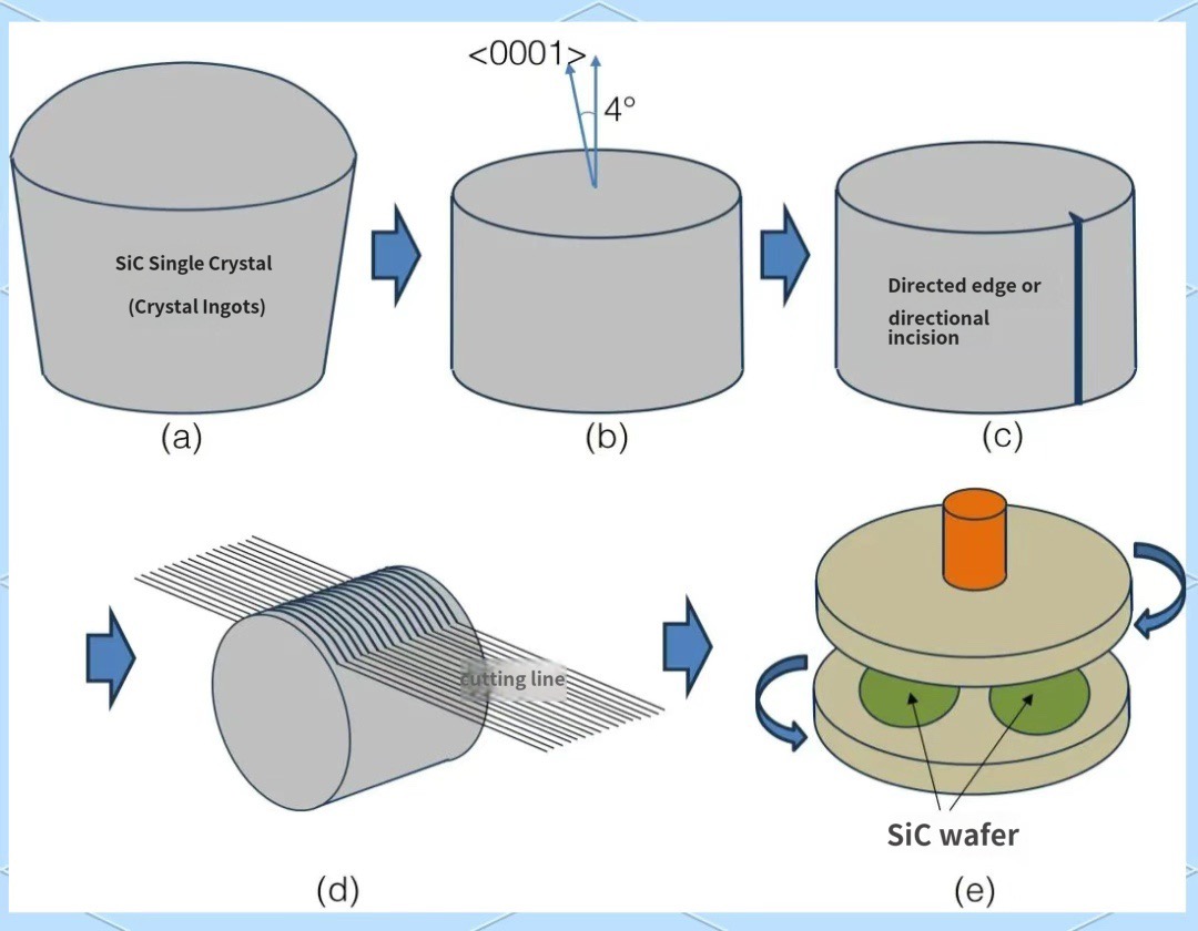
(a) Remove the SiC ingot from the crucible;
(b) Perform initial shaping using outer diameter grinding;
(c) Determine the crystal orientation using alignment flats or notches;
(d) Slice the ingot into thin wafers using multi-wire sawing;
(e) Achieve mirror-like surface smoothness through grinding and polishing steps.
After completing the series of processing steps, the outer edge of the SiC wafer often becomes sharp, which increases the risk of chipping during handling or usage. To avoid such fragility, edge grinding is required.
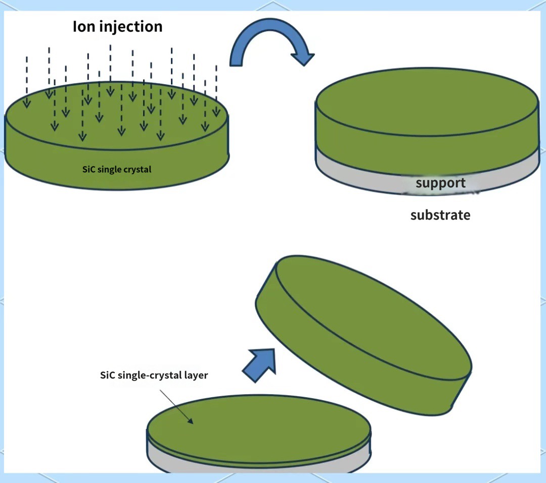
In addition to traditional slicing processes, an innovative method for preparing SiC wafers involves bonding technology. This approach enables wafer fabrication by bonding a thin SiC single-crystal layer to a heterogeneous substrate (supporting substrate).
Figure 3 illustrates the process flow:
First, a delamination layer is formed at a specified depth on the surface of the SiC single crystal via hydrogen ion implantation or similar techniques. The processed SiC single crystal is then bonded to a flat supporting substrate and subjected to pressure and heat. This allows successful transfer and separation of the SiC single-crystal layer onto the supporting substrate.
The separated SiC layer undergoes surface treatment to achieve the required flatness and can be reused in subsequent bonding processes. Compared to traditional slicing of SiC crystals, this technique reduces the demand for expensive materials. Although technical challenges remain, research and development are actively advancing to enable lower-cost wafer production.
Given the high hardness and chemical stability of SiC—which makes it resistant to reactions at room temperature—mechanical polishing is required to remove fine grinding pits, reduce surface damage, eliminate scratches, pitting, and orange peel defects, lower surface roughness, improve flatness, and enhance surface quality.
To achieve a high-quality polished surface, it’s necessary to:
Adjust abrasive types,
Reduce particle size,
Optimize process parameters,
Select polishing materials and pads with adequate hardness.
Figure 7 shows that double-sided polishing with 1 μm abrasives can control flatness and thickness variation within 10 μm, and reduce surface roughness to about 0.25 nm.
3.2 Chemical Mechanical Polishing (CMP)
Chemical Mechanical Polishing (CMP) combines ultrafine particle abrasion with chemical etching to form a smooth, planar surface on the material being processed. The basic principle is:
A chemical reaction occurs between the polishing slurry and the wafer surface, forming a soft layer.
Friction between the abrasive particles and the soft layer removes the material.
CMP advantages:
Overcomes the drawbacks of purely mechanical or chemical polishing,
Achieves both global and local planarization,
Produces surfaces with high flatness and low roughness,
Leaves no surface or subsurface damage.
In detail:
The wafer moves relative to the polishing pad under pressure.
Nanometer-scale abrasives (e.g., SiO₂) in the slurry participate in shearing, weakening Si–C covalent bonds and enhancing material removal.
Types of CMP Techniques:
Free Abrasive Polishing: Abrasives (e.g., SiO₂) are suspended in slurry. Material removal occurs through three-body abrasion (wafer–pad–abrasive). Abrasive size (typically 60–200 nm), pH, and temperature must be precisely controlled to improve uniformity.
Fixed Abrasive Polishing: Abrasives are embedded in the polishing pad to prevent agglomeration—ideal for high-precision processing.
Post-Polishing Cleaning:
Polished wafers undergo:
Chemical cleaning (including DI water and slurry residue removal),
DI water rinsing, and
Hot nitrogen drying
to minimize surface contaminants.
Surface Quality & Performance
Surface roughness can be reduced to Ra < 0.3 nm, meeting semiconductor epitaxy requirements.
Global Planarization: The combination of chemical softening and mechanical removal reduces scratches and uneven etching, outperforming pure mechanical or chemical methods.
High Efficiency: Suitable for hard and brittle materials like SiC, with material removal rates above 200 nm/h.
Other Emerging Polishing Techniques
In addition to CMP, alternative methods have been proposed, including:
Electrochemical polishing,Catalyst-assisted polishing or etching, and
Tribochemical polishing.
However, these methods are still in the research stage and have developed slowly due to SiC’s challenging material properties.
Ultimately, SiC processing is a gradual process of reducing warpage and roughness to improve surface quality, where flatness and roughness control are critical throughout each stage.
Processing Technology
During the wafer grinding stage, diamond slurry with different particle sizes is used to grind the wafer to the required flatness and surface roughness. This is followed by polishing, using both mechanical and chemical mechanical polishing (CMP) techniques to produce damage-free polished silicon carbide (SiC) wafers.
After polishing, the SiC wafers undergo rigorous quality inspection using instruments such as optical microscopes and X-ray diffractometers to ensure all technical parameters meet the required standards. Finally, the polished wafers are cleaned using specialized cleaning agents and ultrapure water to remove surface contaminants. They are then dried using ultra-high purity nitrogen gas and spin dryers, completing the entire production process.
After years of effort, significant progress has been made in SiC single crystal processing within China. Domestically, 100 mm doped semi-insulating 4H-SiC single crystals have been successfully developed, and n-type 4H-SiC and 6H-SiC single crystals can now be produced in batches. Companies like TankeBlue and TYST have already developed 150 mm SiC single crystals.
In terms of SiC wafer processing technology, domestic institutions have preliminarily explored process conditions and routes for crystal slicing, grinding, and polishing. They are capable of producing samples that basically meet the requirements for device fabrication. However, compared to international standards, the surface processing quality of domestic wafers still lags behind significantly. There are several issues:
International SiC theories and processing technologies are tightly protected and not easily accessible.
There is a lack of theoretical research and support for process improvement and optimization.
The cost of importing foreign equipment and components is high.
Domestic research on equipment design, processing precision, and materials still shows significant gaps compared to international levels.
Currently, most high-precision instruments used in China are imported. Testing equipment and methodologies also require further improvement.
With the continued development of third-generation semiconductors, the diameter of SiC single crystal substrates is steadily increasing, along with higher requirements for surface processing quality. Wafer processing technology has become one of the most technically challenging steps after SiC single crystal growth.
To address existing challenges in processing, it is essential to further study the mechanisms involved in cutting, grinding, and polishing, and to explore suitable process methods and routes for SiC wafer manufacturing. At the same time, it is necessary to learn from advanced international processing technologies and adopt state-of-the-art ultra-precision machining techniques and equipment to produce high-quality substrates.
As wafer size increases, the difficulty of crystal growth and processing also rises. However, the manufacturing efficiency of downstream devices improves significantly, and the unit cost is reduced. At present, the main SiC wafer suppliers globally offer products ranging from 4 inches to 6 inches in diameter. Leading companies such as Cree and II-VI have already started planning for the development of 8-inch SiC wafer production lines.
Post time: May-23-2025