Q: What are the main technologies used in SiC wafer slicing and processing?
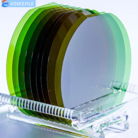
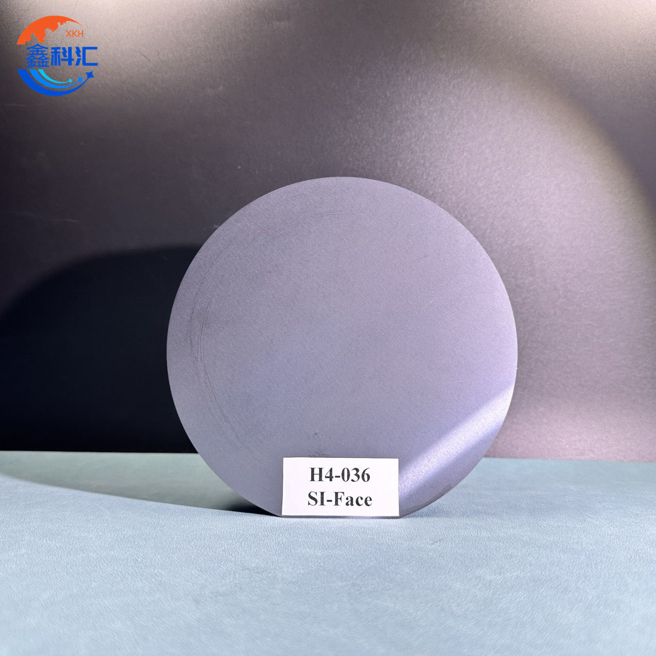
A:Silicon carbide (SiC) has a hardness second only to diamond and is considered a highly hard and brittle material. The slicing process, which involves cutting grown crystals into thin wafers, is time-consuming and prone to chipping. As the first step in SiC single crystal processing, the quality of slicing significantly influences subsequent grinding, polishing, and thinning. Slicing often introduces surface and subsurface cracks, increasing wafer breakage rates and production costs. Therefore, controlling surface crack damage during slicing is crucial to advancing SiC device fabrication.
Currently reported SiC slicing methods include fixed-abrasive, free-abrasive slicing, laser cutting, layer transfer (cold separation), and electrical discharge slicing. Among these, reciprocating multi-wire slicing with fixed diamond abrasives is the most commonly used method for processing SiC single crystals. However, as ingot sizes reach 8 inches and above, traditional wire sawing becomes less practical due to high equipment demands, costs, and low efficiency. There is an urgent need for low-cost, low-loss, high-efficiency slicing technologies.
Q: What are the advantages of laser slicing over traditional multi-wire cutting?
A:Traditional wire sawing cuts the SiC ingot along a specific direction into slices several hundred microns thick. The slices are then ground using diamond slurries to remove saw marks and subsurface damage, followed by chemical mechanical polishing (CMP) to achieve global planarization, and finally cleaned to obtain SiC wafers.
However, due to SiC's high hardness and brittleness, these steps can easily cause warping, cracking, increased breakage rates, higher production costs, and result in high surface roughness and contamination (dust, wastewater, etc.). Additionally, wire sawing is slow and has a low yield. Estimates show that traditional multi-wire slicing achieves only about 50% material utilization, and up to 75% of the material is lost after polishing and grinding. Early foreign production data indicated that it could take approximately 273 days of continuous 24-hour production to produce 10,000 wafers—very time-intensive.
Domestically, many SiC crystal growth companies are focused on increasing furnace capacity. However, instead of just expanding output, it is more important to consider how to reduce losses—especially when crystal growth yields are not yet optimal.
Laser slicing equipment can significantly reduce material loss and improve yield. For example, using a single 20 mm SiC ingot:Wire sawing can yield around 30 wafers of 350 μm thickness.Laser slicing can yield more than 50 wafers.If wafer thickness is reduced to 200 μm, more than 80 wafers can be produced from the same ingot.While wire sawing is widely used for wafers 6 inches and smaller, slicing an 8-inch SiC ingot may take 10–15 days with traditional methods, requiring high-end equipment and incurring high costs with low efficiency. Under these conditions, laser slicing's advantages become clear, making it the mainstream future technology for 8-inch wafers.
With laser cutting, the slicing time per 8-inch wafer can be under 20 minutes, with material loss per wafer under 60 μm.
In summary, compared to multi-wire cutting, laser slicing offers higher speed, better yield, lower material loss, and cleaner processing.
Q: What are the main technical challenges in SiC laser slicing?
A:The laser slicing process involves two main steps: laser modification and wafer separation.
The core of laser modification is beam shaping and parameter optimization. Parameters such as laser power, spot diameter, and scan speed all affect the quality of material ablation and the success of subsequent wafer separation. The geometry of the modified zone determines surface roughness and the difficulty of separation. High surface roughness complicates later grinding and increases material loss.
After modification, wafer separation is typically achieved through shear forces, such as cold fracture or mechanical stress. Some domestic systems use ultrasonic transducers to induce vibrations for separation, but this can cause chipping and edge defects, lowering the final yield.
While these two steps are not inherently difficult, inconsistencies in crystal quality—due to different growth processes, doping levels, and internal stress distributions—significantly affect slicing difficulty, yield, and material loss. Merely identifying problem areas and adjusting laser scanning zones may not substantially improve results.
The key to widespread adoption lies in developing innovative methods and equipment that can adapt to a wide range of crystal qualities from various manufacturers, optimizing process parameters, and building laser slicing systems with universal applicability.
Q: Can laser slicing technology be applied to other semiconductor materials besides SiC?
A:Laser cutting technology has historically been applied to a wide range of materials. In semiconductors, it was initially used for wafer dicing and has since expanded to slicing large bulk single crystals.
Beyond SiC, laser slicing can also be used for other hard or brittle materials such as diamond, gallium nitride (GaN), and gallium oxide (Ga₂O₃). Preliminary studies on these materials have demonstrated the feasibility and advantages of laser slicing for semiconductor applications.
Q: Are there currently mature domestic laser slicing equipment products? What stage is your research in?
A:Large-diameter SiC laser slicing equipment is widely considered core equipment for the future of 8-inch SiC wafer production. Currently, only Japan can provide such systems, and they are expensive and subject to export restrictions.
Domestic demand for laser slicing/thinning systems is estimated to be around 1,000 units, based on SiC production plans and existing wire saw capacity. Major domestic companies have invested heavily in development, but no mature, commercially available domestic equipment has yet reached industrial deployment.
Research groups have been developing proprietary laser lift-off technology since 2001 and have now extended this to large-diameter SiC laser slicing and thinning. They have developed a prototype system and slicing processes capable of:Cutting and thinning 4–6 inch semi-insulating SiC wafersSlicing 6–8 inch conductive SiC ingotsPerformance benchmarks:6–8 inch semi-insulating SiC: slicing time 10–15 minutes/wafer; material loss <30 μm6–8 inch conductive SiC: slicing time 14–20 minutes/wafer; material loss <60 μm
Estimated wafer yield increased by over 50%
Post-slicing, the wafers meet national standards for geometry after grinding and polishing. Studies also show that laser-induced thermal effects do not significantly impact stress or geometry in the wafers.
The same equipment has also been used to verify feasibility for slicing diamond, GaN, and Ga₂O₃ single crystals.
Post time: May-23-2025