High-Purity Fused Quartz Wafers for Semiconductor, Photonics Optical Applications 2″4″6″8″12″


Detailed Diagram


Overview of Quartz Glass
Quartz wafers form the backbone of countless modern devices that drive today’s digital world. From the navigation in your smartphone to the backbone of 5G base stations, quartz quietly delivers the stability, purity, and precision required in high-performance electronics and photonics. Whether supporting flexible circuitry, enabling MEMS sensors, or forming the basis for quantum computing, quartz’s unique characteristics make it indispensable across industries.
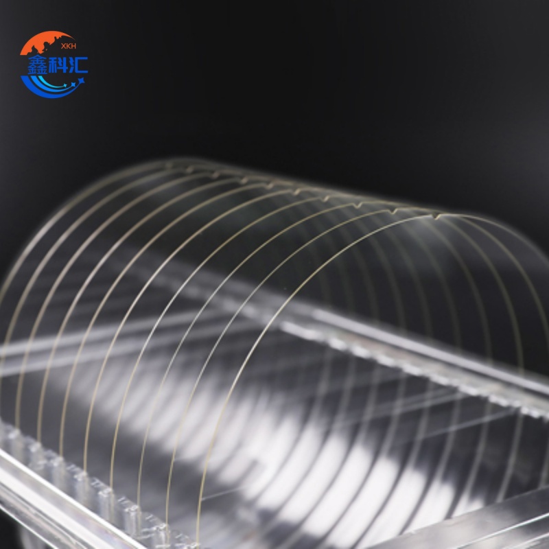
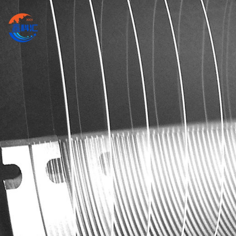
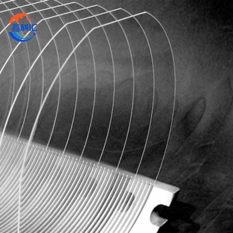
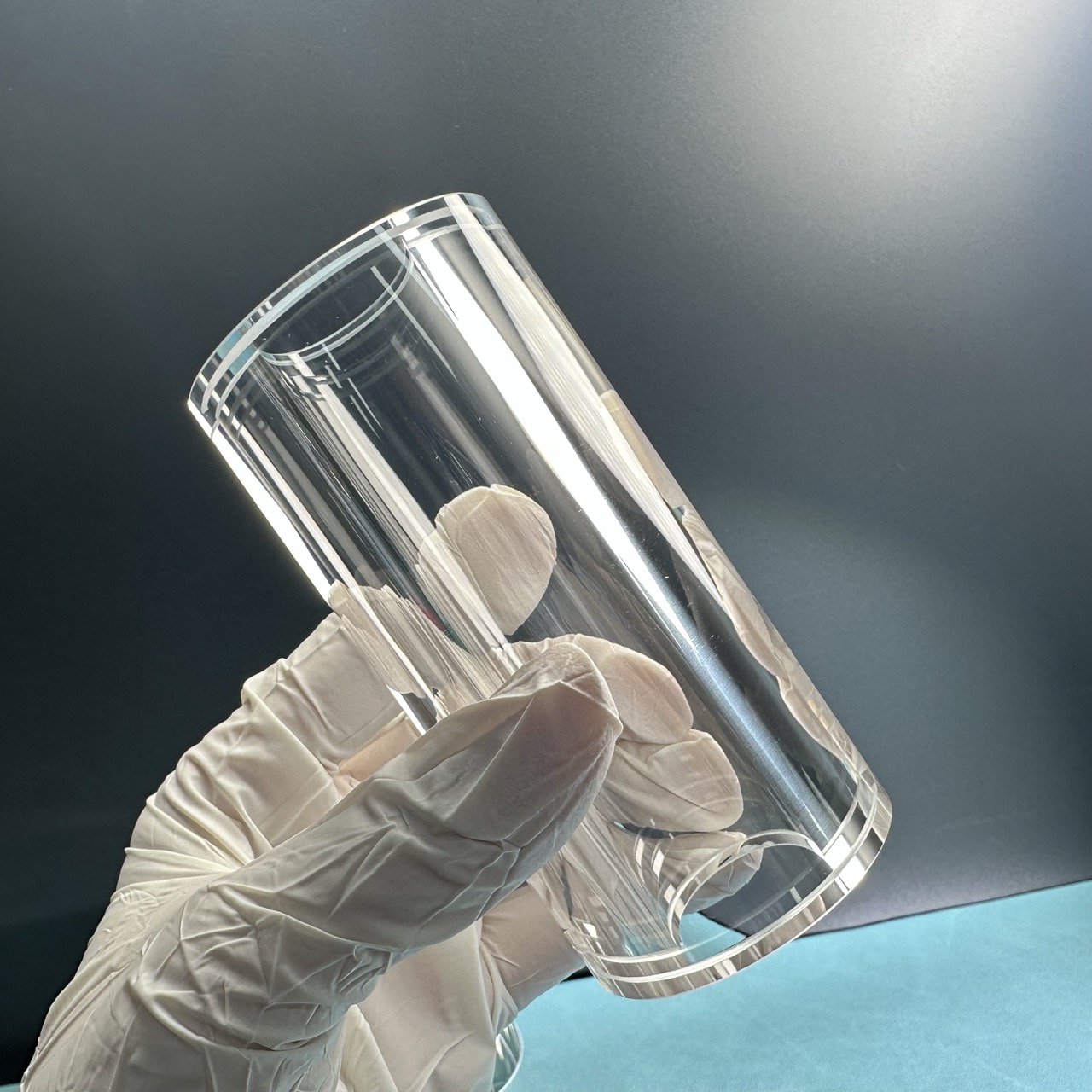
“Fused Silica” or “Fused Quartz” which is the amorphous phase of quartz (SiO2). When contrasted to borosilicate glass, fused silica has no additives; hence it exists in its pure form, SiO2. Fused silica has a higher transmission in the infrared and ultraviolet spectrum when compared to normal glass. Fused silica is produced by melting and re-solidifying ultrapure SiO2. Synthetic fused silica on the other hand is made from silicon-rich chemical precursors such as SiCl4 which are gasified and then oxidized in a H2 + O2 atmosphere. The SiO2 dust formed in this case is fused to silica on a substrate. The fused silica blocks are cut into wafers after which the wafers are finally polished.
Key Features and Benefits of Quartz Glass Wafer
-
Ultra-High Purity (≥99.99% SiO2)
Ideal for ultra-clean semiconductor and photonics processes where material contamination must be minimized. -
Wide Thermal Operating Range
Maintains structural integrity from cryogenic temperatures up to over 1100°C without warping or degradation. -
Outstanding UV and IR Transmission
Delivers excellent optical clarity from deep ultraviolet (DUV) through near-infrared (NIR), supporting precision optical applications. -
Low Thermal Expansion Coefficient
Enhances dimensional stability under temperature fluctuations, reducing stress and improving process reliability. -
Superior Chemical Resistance
Inert to most acids, alkalis, and solvents—making it well-suited for chemically aggressive environments. -
Surface Finish Flexibility
Available with ultra-smooth, single-side or double-side polished finishes, compatible with photonics and MEMS requirements.
Manufacturing Process of Quartz Glass Wafer
Fused quartz wafers are produced via a series of controlled and precise steps:
-
Raw Material Selection
Selection of high-purity natural quartz or synthetic SiO₂ sources. -
Melting and Fusion
Quartz is melted at ~2000°C in electric furnaces under a controlled atmosphere to eliminate inclusions and bubbles. -
Block Forming
The molten silica is cooled into solid blocks or ingots. -
Wafer Slicing
Precision diamond or wire saws are used to cut the ingots into wafer blanks. -
Lapping & Polishing
Both surfaces are flattened and polished to meet exact optical, thickness, and roughness specifications. -
Cleaning & Inspection
Wafers are cleaned in ISO Class 100/1000 cleanrooms and subjected to rigorous inspection for defects and dimensional conformity.
Properties of Quartz Glass wafer
| spec | unit | 4" | 6" | 8" | 10" | 12" |
|---|---|---|---|---|---|---|
| Diameter / size (or square) | mm | 100 | 150 | 200 | 250 | 300 |
| Tolerance (±) | mm | 0.2 | 0.2 | 0.2 | 0.2 | 0.2 |
| Thickness | mm | 0.10 or more | 0.30 or more | 0.40 or more | 0.50 or more | 0.50 or more |
| Primary reference flat | mm | 32.5 | 57.5 | Semi-notch | Semi-notch | Semi-notch |
| LTV (5mm×5mm) | μm | < 0.5 | < 0.5 | < 0.5 | < 0.5 | < 0.5 |
| TTV | μm | < 2 | < 3 | < 3 | < 5 | < 5 |
| Bow | μm | ±20 | ±30 | ±40 | ±40 | ±40 |
| Warp | μm | ≤ 30 | ≤ 40 | ≤ 50 | ≤ 50 | ≤ 50 |
| PLTV (5mm×5mm) < 0.4μm | % | ≥95% | ≥95% | ≥95% | ≥95% | ≥95% |
| Edge Rounding | mm | Compliant with SEMI M1.2 Standard / refer to IEC62276 | ||||
| Surface Type | Single Side Polished / Double Sides Polished | |||||
| Polished side Ra | nm | ≤1 | ≤1 | ≤1 | ≤1 | ≤1 |
| Back Side Criteria | μm | general 0.2-0.7 or customized | ||||
Quartz vs. Other Transparent Materials
| Property | Quartz Glass | Borosilicate Glass | Sapphire | Standard Glass |
|---|---|---|---|---|
| Max Operating Temp | ~1100°C | ~500°C | ~2000°C | ~200°C |
| UV Transmission | Excellent (JGS1) | Poor | Good | Very poor |
| Chemical Resistance | Excellent | Moderate | Excellent | Poor |
| Purity | Extremely high | Low to moderate | High | Low |
| Thermal Expansion | Very low | Moderate | Low | High |
| Cost | Moderate to high | Low | High | Very low |
FAQ of Quartz Glass Wafer
Q1: What’s the difference between fused quartz and fused silica?
While both are amorphous forms of SiO₂, fused quartz typically originates from natural quartz sources, whereas fused silica is synthetically produced. Functionally, they offer similar performance, but fused silica may have slightly higher purity and homogeneity.
Q2: Can fused quartz wafers be used in high-vacuum environments?
Yes. Due to their low outgassing properties and high thermal resistance, fused quartz wafers are excellent for vacuum systems and aerospace applications.
Q3: Are these wafers suitable for deep-UV laser applications?
Absolutely. Fused quartz has high transmittance down to ~185 nm, making it ideal for DUV optics, lithography masks, and excimer laser systems.
Q4: Do you support custom wafer fabrication?
Yes. We offer full customization including diameter, thickness, surface quality, flats/notches, and laser patterning, based on your specific application requirements.
About Us
XKH specializes in high-tech development, production, and sales of special optical glass and new crystal materials. Our products serve optical electronics, consumer electronics, and the military. We offer Sapphire optical components, mobile phone lens covers, Ceramics, LT, Silicon Carbide SIC, Quartz, and semiconductor crystal wafers. With skilled expertise and cutting-edge equipment, we excel in non-standard product processing, aiming to be a leading optoelectronic materials high-tech enterprise.

Related Products
-
Sapphire Rods Industrial Applications sapphire ...
-

Synthetic Sapphire boule Monocrystal Sapphire B...
-

Sapphire Tube Unpolished Small Size Al2O3 Glass...
-

Lens Prism Optical Glass DSP Custom Size 99.999...
-

Sapphire Single Crystal Ingot ky method Al2O3
-

Single Crystal Ruby Rod for Medicine, industry,...