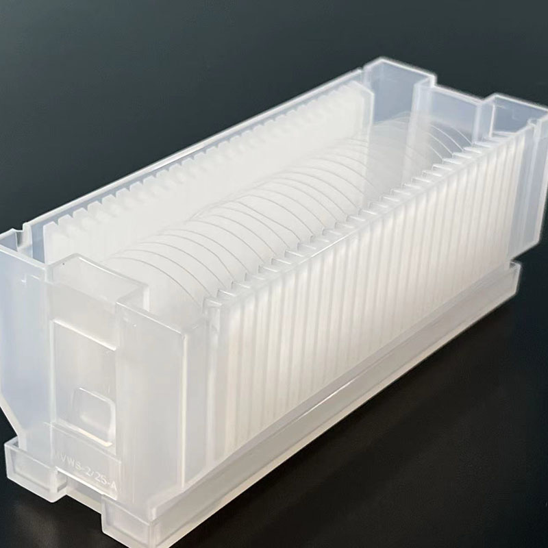
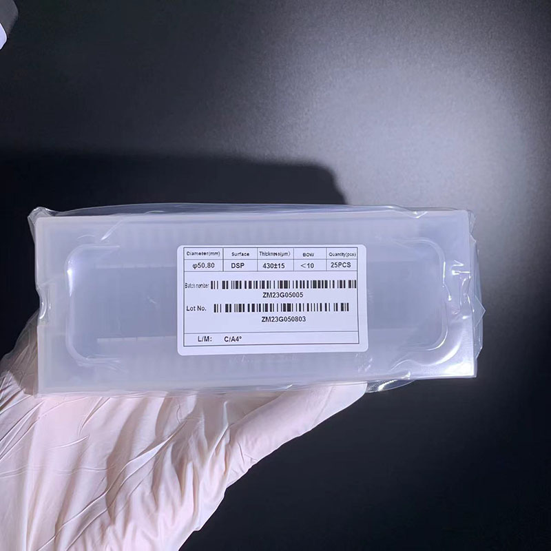
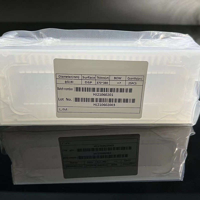
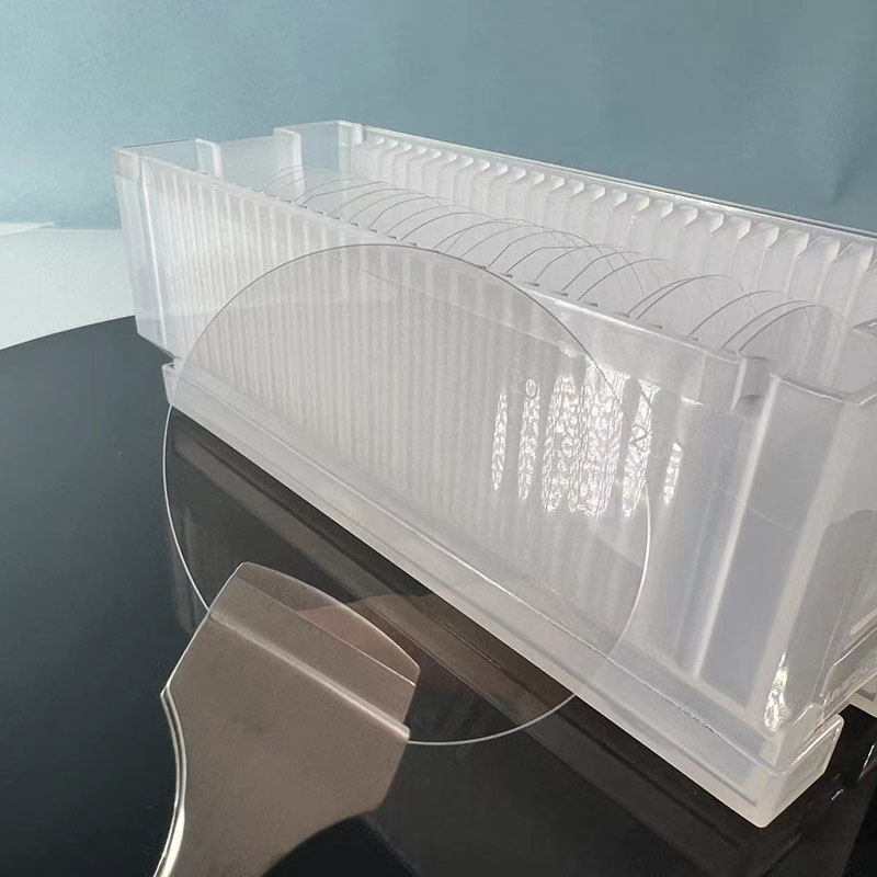
Dia50.8×0.1/0.17/0.2/0.25/0.3mmt Sapphire Wafer substrate Epi-ready DSP SSP

Below is the 2inch Sapphire Wafer description, nature advantages, general use and standard wafer parameter index about 2-inch sapphire wafers:
Product Description: 2 inch sapphire wafers are made by cutting the sapphire single crystal material into a silicon wafer shape with a smooth and flat surface. It is a very stable and durable material widely used in optics, electronics and photonics.
Properties Advantages
High hardness: Sapphire has a Mohs hardness level of 9, second only to diamond, resulting in excellent scratch and wear resistance.
High melting point: Sapphire has a melting point of approximately 2040°C, enabling it to work in high-temperature environments with excellent thermal stability.
Chemical stability: Sapphire has excellent chemical stability and is resistant to acids, alkalis and corrosive gases, making it suitable for applications in a variety of harsh environments.
General Use
Optical applications: sapphire wafers can be used in laser systems, optical windows, lenses, infrared optics devices, and more. Because of its excellent transparency, sapphire is widely used in the optical field.
Electronic applications: Sapphire wafers can be used in the manufacture of diodes, LEDs, laser diodes and other electronic devices. Sapphire has excellent thermal conductivity and electrical insulation properties, suitable for high-power electronic devices.
Optoelectronic applications: Sapphire wafers can be used to manufacture image sensors, photodetectors and other optoelectronic devices. Sapphire's low loss and high response properties make it ideal for optoelectronic applications.
Standard wafer parameter specifications:
Diameter: 2 inches (approximately 50.8 mm)
Thickness: Common thicknesses include 0.5 mm, 1.0 mm, and 2.0 mm. Other thicknesses can be customized upon request.
Surface roughness: Generally Ra < 0.5 nm.
Double-sided polishing: flatness is typically < 10 µm.
Double-sided polished single crystal sapphire wafers: wafers polished on both sides and with a higher degree of parallelism for applications requiring higher requirements.
Please note that specific product parameters may vary depending on the requirements of the manufacturer and the application.
Detailed Diagram