6 inch-8 inch LN-on-Si Composite Substrate Thickness 0.3-50 μm Si/SiC/Sapphire of Materials


Technical parameters
|
0.3-50μm LN/LT on Insulators |
|
|
Top layer |
|
|
Diameter |
6-8 inch |
|
Orientation |
X, Z, Y-42 etc. |
|
Materials |
LT, LN |
|
Thickness |
0.3-50μm |
|
Substrate(Customized) |
|
|
Material |
Si, SiC, Sapphire, Spinel, Quartz |
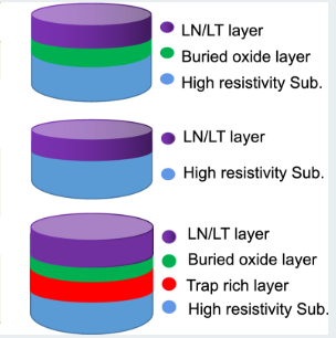
Key Features
The 6-inch to 8-inch LN-on-Si composite substrate is distinguished by its unique material properties and tunable parameters, enabling broad applicability in semiconductor and optoelectronic industries:
1.Large Wafer Compatibility: The 6-inch to 8-inch wafer size ensures seamless integration with existing semiconductor fabrication lines (e.g., CMOS processes), reducing production costs and enabling mass production.
2.High Crystalline Quality: Optimized epitaxial or bonding techniques ensure low defect density in the LN thin film, making it ideal for high-performance optical modulators, surface acoustic wave (SAW) filters, and other precision devices.
3.Adjustable Thickness (0.3–50 μm): Ultrathin LN layers (<1 μm) are suitable for integrated photonic chips, while thicker layers (10–50 μm) support high-power RF devices or piezoelectric sensors.
4.Multiple Substrate Options: In addition to Si, SiC (high thermal conductivity) or sapphire (high insulation) can be selected as base materials to meet the demands of high-frequency, high-temperature, or high-power applications.
5.Thermal and Mechanical Stability: The silicon substrate provides robust mechanical support, minimizing warping or cracking during processing and improving device yield.
These attributes position the 6-inch to 8-inch LN-on-Si composite substrate as a preferred material for cutting-edge technologies such as 5G communications, LiDAR, and quantum optics.
Main Applications
The 6-inch to 8-inch LN-on-Si composite substrate is widely adopted in high-tech industries due to its exceptional electro-optic, piezoelectric, and acoustic properties:
1.Optical Communications and Integrated Photonics: Enables high-speed electro-optic modulators, waveguides, and photonic integrated circuits (PICs), addressing the bandwidth demands of data centers and fiber-optic networks.
2.5G/6G RF Devices: The high piezoelectric coefficient of LN makes it ideal for surface acoustic wave (SAW) and bulk acoustic wave (BAW) filters, enhancing signal processing in 5G base stations and mobile devices.
3.MEMS and Sensors: The piezoelectric effect of LN-on-Si facilitates high-sensitivity accelerometers, biosensors, and ultrasonic transducers for medical and industrial applications.
4.Quantum Technologies: As a nonlinear optical material, LN thin films are used in quantum light sources (e.g., entangled photon pairs) and integrated quantum chips.
5.Lasers and Nonlinear Optics: Ultrathin LN layers enable efficient second-harmonic generation (SHG) and optical parametric oscillation (OPO) devices for laser processing and spectroscopic analysis.
The standardized 6-inch to 8-inch LN-on-Si composite substrate allows these devices to be manufactured in large-scale wafer fabs, significantly reducing production costs.
Customization and Services
We provide comprehensive technical support and customization services for the 6-inch to 8-inch LN-on-Si composite substrate to meet diverse R&D and production needs:
1.Custom Fabrication: LN film thickness (0.3–50 μm), crystal orientation (X-cut/Y-cut), and substrate material (Si/SiC/sapphire) can be tailored to optimize device performance.
2.Wafer-Level Processing: Bulk supply of 6-inch and 8-inch wafers, including back-end services such as dicing, polishing, and coating, ensuring substrates are ready for device integration.
3.Technical Consultation and Testing: Material characterization (e.g., XRD, AFM), electro-optic performance testing, and device simulation support to expedite design validation.
Our mission is to establish the 6-inch to 8-inch LN-on-Si composite substrate as a core material solution for optoelectronic and semiconductor applications, offering end-to-end support from R&D to mass production.
Conclusion
The 6-inch to 8-inch LN-on-Si composite substrate, with its large wafer size, superior material quality, and versatility, is driving advancements in optical communications, 5G RF, and quantum technologies. Whether for high-volume manufacturing or customized solutions, we deliver reliable substrates and complementary services to empower technological innovation.
Related Products
-

4 inch Sapphire Wafer C-Plane SSP/DSP 0.43mm 0....
-

Au coated wafer,sapphire wafer,silicon wafer...
-

2inch Silicon Carbide Wafer 6H-N Type Prime Gra...
-
Sapphire green for gemstone olive green artific...
-

Al2O3 sapphire tube,Sapphire Capillary tube,R...
-

Sapphire blade for hair transplant 0.8mm 1.0mm ...