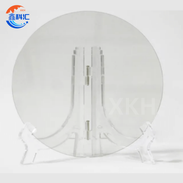
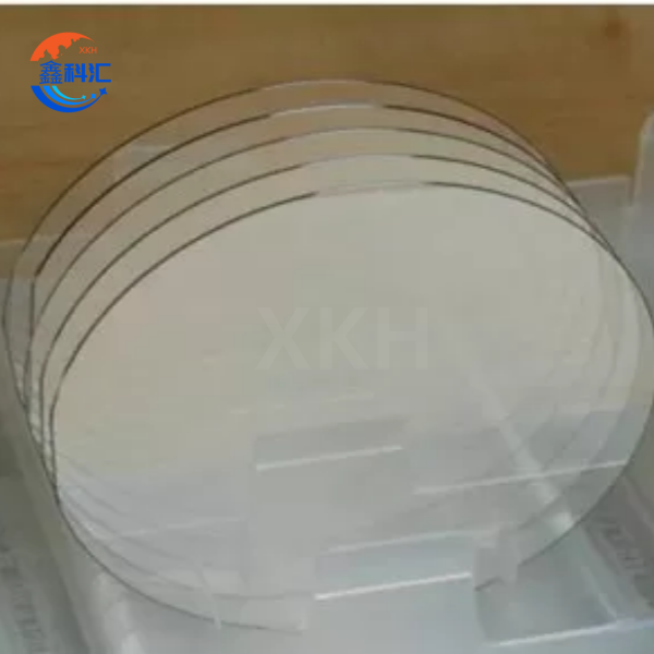
6 Inch 4H SEMI Type SiC composite substrate Thickness 500μm TTV≤5μm MOS grade


Technical parameters
|
Items |
Specification |
Items |
Specification |
|
Diameter |
150±0.2 mm |
Front (Si-face) roughness |
Ra≤0.2 nm (5μm×5μm) |
|
Polytype |
4H |
Edge Chip, Scratch, Crack (visual inspection) |
None |
|
Resistivity |
≥1E8 Ω·cm |
TTV |
≤5 μm |
|
Transfer layer Thickness |
≥0.4 μm |
Warp |
≤35 μm |
|
Void (2mm>D>0.5mm) |
≤5 ea/Wafer |
Thickness |
500±25 μm |
Key Features
1. Exceptional High-Frequency Performance
The 6-inch semi-insulating SiC composite substrate employs a graded dielectric layer design, ensuring dielectric constant variation of <2% in the Ka-band (26.5-40 GHz) and improving phase consistency by 40%. 15% increase in efficiency and 20% lower power consumption in T/R modules using this substrate.
2. Breakthrough Thermal Management
A unique "thermal bridge" composite structure enables lateral thermal conductivity of 400 W/m·K. In 28 GHz 5G base station PA modules, the junction temperature rises by only 28°C after 24 hours of continuous operation—50°C lower than conventional solutions.
3. Superior Wafer Quality
Through an optimized Physical Vapor Transport (PVT) method, we achieve dislocation density <500/cm² and Total Thickness Variation (TTV) <3 μm.
4. Manufacturing-Friendly Processing
Our laser annealing process specifically developed for the 6-inch semi-insulating SiC composite substrate reduces surface state density by two orders of magnitude before epitaxy.
Main Applications
1. 5G Base Station Core Components
In Massive MIMO antenna arrays, GaN HEMT devices on 6-inch semi-insulating SiC composite substrates achieve 200W output power and >65% efficiency. Field tests at 3.5 GHz showed a 30% increase in coverage radius.
2. Satellite Communication Systems
Low-Earth orbit (LEO) satellite transceivers using this substrate exhibit 8 dB higher EIRP in the Q-band (40 GHz) while reducing weight by 40%. SpaceX Starlink terminals have adopted it for mass production.
3. Military Radar Systems
Phased-array radar T/R modules on this substrate achieve 6-18 GHz bandwidth and noise figure as low as 1.2 dB, extending detection range by 50 km in early-warning radar systems.
4. Automotive Millimeter-Wave Radar
79 GHz automotive radar chips using this substrate improve angular resolution to 0.5°, meeting L4 autonomous driving requirements.
We offer a comprehensive customized service solution for 6-inch semi-insulating SiC composite substrates. In terms of customizing material parameters, we support precise regulation of resistivity within the range of 10⁶-10¹⁰ Ω·cm. Particularly for military applications, we can offer an ultra-high resistance option of >10⁹ Ω·cm. It offers three thickness specifications of 200μm, 350μm and 500μm simultaneously, with the tolerance strictly controlled within ±10μm, meeting different requirements from high-frequency devices to high-power applications.
In terms of surface treatment processes, we offer two professional solutions: Chemical Mechanical Polishing (CMP) can achieve atomic-level surface flatness with Ra<0.15nm, meeting the most demanding epitaxial growth requirements; The epitaxial ready surface treatment technology for rapid production demands can provide ultra-smooth surfaces with Sq<0.3nm and residual oxide thickness <1nm, significantly simplifying the pretreatment process at the client's end.
XKH provides comprehensive customized solutions for 6-inch semi-insulating SiC composite substrates
1. Material Parameter Customization
We offer precise resistivity tuning within the range of 10⁶-10¹⁰ Ω·cm, with specialized ultra-high resistivity options >10⁹ Ω·cm available for military/aerospace applications.
2. Thickness Specifications
Three standardized thickness options:
· 200μm (optimized for high-frequency devices)
· 350μm (standard specification)
· 500μm (designed for high-power applications)
· All variants maintain tight thickness tolerances of ±10μm.
3. Surface Treatment Technologies
Chemical Mechanical Polishing (CMP): Achieves atomic-level surface flatness with Ra<0.15nm, meeting stringent epitaxial growth requirements for RF and power devices.
4. Epi-Ready Surface Processing
· Delivers ultra-smooth surfaces with Sq<0.3nm roughness
· Controls native oxide thickness to <1nm
· Eliminates up to 3 pre-processing steps at customer facilities
Related Products
-
SiC ceramic tray plate graphite with CVD SiC co...
-

Silicon Carbide Ceramic Tray – Durable, High-Pe...
-

SICOI (Silicon Carbide on Insulator) Wafers SiC...
-

Sapphire Square Seed Crystal – Precision-Orient...
-

Alumina ceramic arm custom Ceramic robotic arm
-

High Performance Sapphire Step Window, Al2O3 Si...