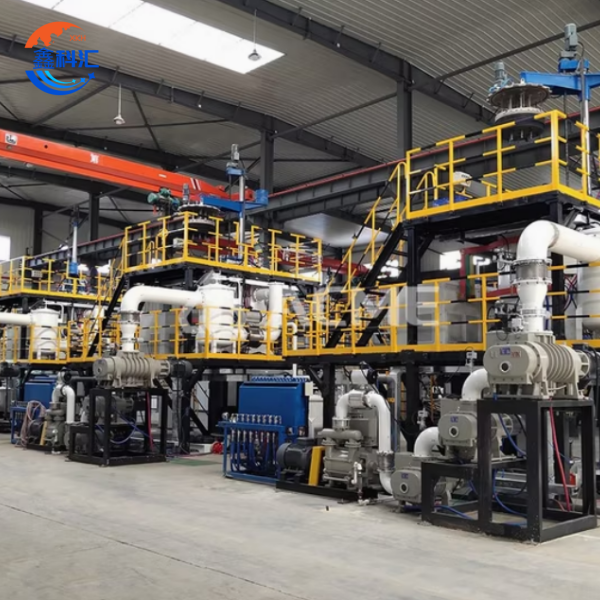
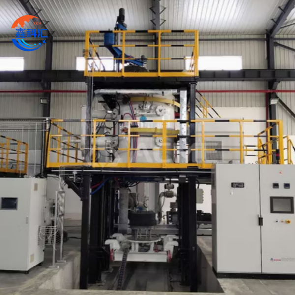
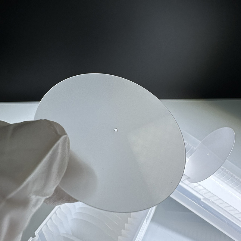
4inch 6inch 8inch SiC Crystal Growth Furnace for CVD Process


Working Principle
The core principle of our CVD system involves thermal decomposition of silicon-containing (e.g., SiH4) and carbon-containing (e.g., C3H8) precursor gases at high temperatures (typically 1500-2000°C), depositing SiC single crystals on substrates through gas-phase chemical reactions. This technology is especially suitable for producing high-purity (>99.9995%) 4H/6H-SiC single crystals with low defect density (<1000/cm²), meeting stringent material requirements for power electronics and RF devices. Through precise control of gas composition, flow rate and temperature gradient, the system enables accurate regulation of crystal conductivity type (N/P type) and resistivity.
System Types and Technical Parameters
| System Type | Temperature Range | Key Features | Applications |
| High-Temp CVD | 1500-2300°C | Graphite induction heating, ±5°C temperature uniformity | Bulk SiC crystal growth |
| Hot-Filament CVD | 800-1400°C | Tungsten filament heating, 10-50μm/h deposition rate | SiC thick epitaxy |
| VPE CVD | 1200-1800°C | Multi-zone temperature control, >80% gas utilization | Mass epi-wafer production |
| PECVD | 400-800°C | Plasma enhanced, 1-10μm/h deposition rate | Low-temp SiC thin films |
Key Technical Characteristics
1. Advanced Temperature Control System
The furnace features a multi-zone resistive heating system capable of maintaining temperatures up to 2300°C with ±1°C uniformity across the entire growth chamber. This precision thermal management is achieved through:
12 independently controlled heating zones.
Redundant thermocouple monitoring (Type C W-Re).
Real-time thermal profile adjustment algorithms.
Water-cooled chamber walls for thermal gradient control.
2. Gas Delivery and Mixing Technology
Our proprietary gas distribution system ensures optimal precursor mixing and uniform delivery:
Mass flow controllers with ±0.05sccm accuracy.
Multi-point gas injection manifold.
In-situ gas composition monitoring (FTIR spectroscopy).
Automatic flow compensation during growth cycles.
3. Crystal Quality Enhancement
The system incorporates several innovations to improve crystal quality:
Rotating substrate holder (0-100rpm programmable).
Advanced boundary layer control technology.
In-situ defect monitoring system (UV laser scattering).
Automatic stress compensation during growth.
4. Process Automation and Control
Fully automated recipe execution.
Real-time growth parameter optimization AI.
Remote monitoring and diagnostics.
1000+ parameter data logging (stored for 5 years).
5. Safety and Reliability Features
Triple-redundant over-temperature protection.
Automatic emergency purge system.
Seismic-rated structural design.
98.5% uptime guarantee.
6. Scalable Architecture
Modular design allows capacity upgrades.
Compatible with 100mm to 200mm wafer sizes.
Supports both vertical and horizontal configurations.
Quick-change components for maintenance.
7. Energy Efficiency
30% lower power consumption than comparable systems.
Heat recovery system captures 60% of waste heat.
Optimized gas consumption algorithms.
LEED-compliant facility requirements.
8. Material Versatility
Grows all major SiC polytypes (4H, 6H, 3C).
Supports both conductive and semi-insulating variants.
Accommodates various doping schemes (N-type, P-type).
Compatible with alternative precursors (e.g., TMS, TES).
9. Vacuum System Performance
Base pressure: <1×10⁻⁶ Torr
Leak rate: <1×10⁻⁹ Torr·L/sec
Pumping speed: 5000L/s (for SiH₄)
Automatic pressure control during growth cycles
This comprehensive technical specification demonstrates our system's capability to produce research-grade and production-quality SiC crystals with industry-leading consistency and yield. The combination of precision control, advanced monitoring, and robust engineering makes this CVD system the optimal choice for both R&D and volume manufacturing applications in power electronics, RF devices, and other advanced semiconductor applications.
Key Advantages
1. High-Quality Crystal Growth
• Defect density as low as <1000/cm² (4H-SiC)
• Doping uniformity <5% (6-inch wafers)
• Crystal purity >99.9995%
2. Large-Size Production Capability
• Supports up to 8-inch wafer growth
• Diameter uniformity >99%
• Thickness variation <±2%
3. Precise Process Control
• Temperature control accuracy ±1°C
• Gas flow control accuracy ±0.1sccm
• Pressure control accuracy ±0.1Torr
4. Energy Efficiency
• 30% more energy efficient than conventional methods
• Growth rate up to 50-200μm/h
• Equipment uptime >95%
Key Applications
1. Power Electronic Devices
6-inch 4H-SiC substrates for 1200V+ MOSFETs/diodes, reducing switching losses by 50%.
2. 5G Communication
Semi-insulating SiC substrates (resistivity >10⁸Ω·cm) for base station PAs, with insertion loss <0.3dB at >10GHz.
3. New Energy Vehicles
Automotive-grade SiC power modules extend EV range by 5-8% and reduce charging time by 30%.
4. PV Inverters
Low-defect substrates boost conversion efficiency beyond 99% while reducing system size by 40%.
XKH's Services
1. Customization Services
Tailored 4-8 inch CVD systems.
Supports growth of 4H/6H-N type, 4H/6H-SEMI insulating type, etc.
2. Technical Support
Comprehensive training on operation and process optimization.
24/7 technical response.
3. Turnkey Solutions
End-to-end services from installation to process validation.
4. Material Supply
2-12 inch SiC substrates/epi-wafers available.
Supports 4H/6H/3C polytypes.
Key differentiators include:
Up to 8-inch crystal growth capability.
20% faster growth rate than industry average.
98% system reliability.
Full intelligent control system package.
Related Products
-

Sapphire Square Blank Substrate – Optical, Semi...
-
Transparent Custom Sapphire Watchcase: Fashiona...
-
Surface processing method of titanium-doped sap...
-

sapphire ingot 3inch 4inch 6inch Monocrystal CZ...
-

UV Laser Marking Machine Plastic Glass PCB Cold...
-
Customised Sapphire small Square Hole Punching ...