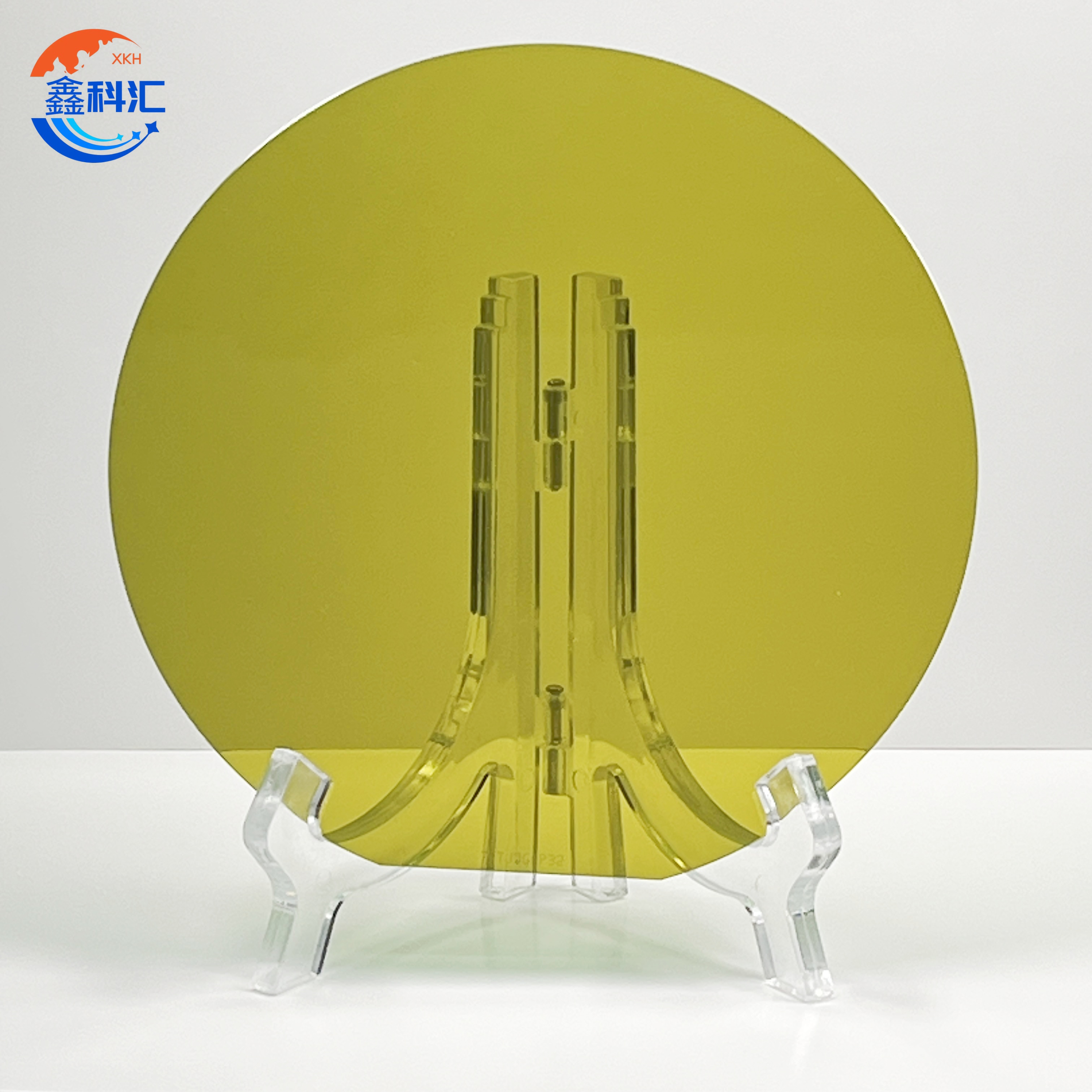
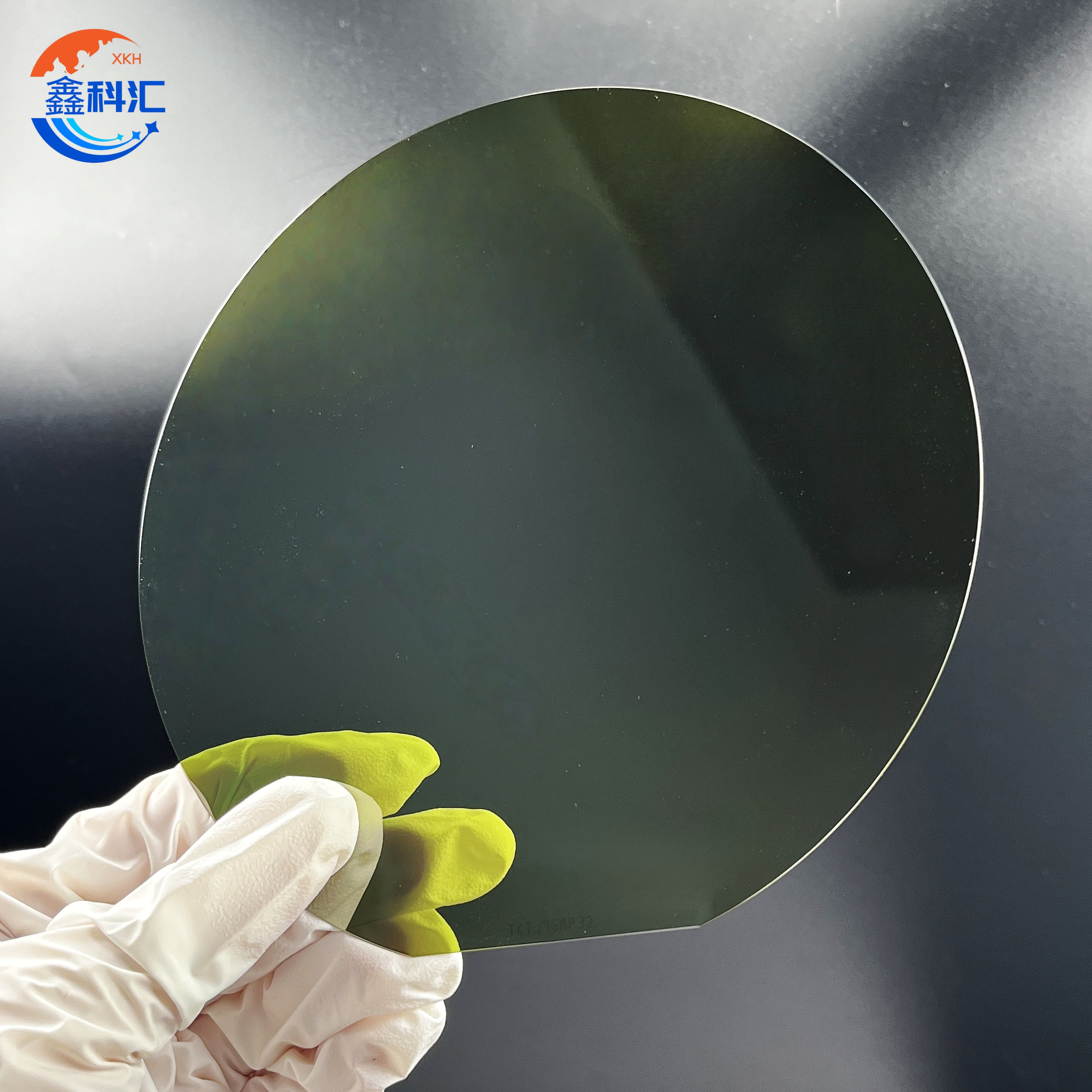
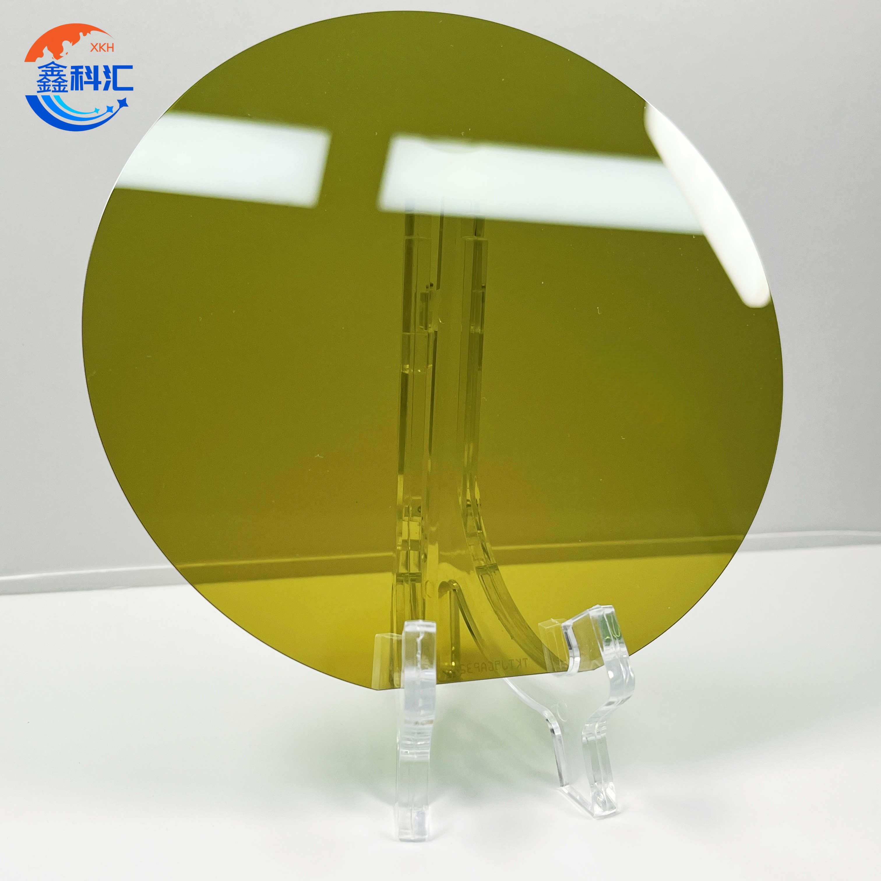
4H-SiC Epitaxial Wafers for Ultra-High Voltage MOSFETs (100–500 μm, 6 inch)


Detailed Diagram


Product Overview
The rapid growth of electric vehicles, smart grids, renewable energy systems, and high-power industrial equipment has created an urgent need for semiconductor devices capable of handling higher voltages, higher power densities, and greater efficiency. Among wide bandgap semiconductors, silicon carbide (SiC) stands out for its wide bandgap, high thermal conductivity, and superior critical electric field strength.
Our 4H-SiC epitaxial wafers are engineered specifically for ultra-high voltage MOSFET applications. With epitaxial layers ranging from 100 μm to 500 μm on 6-inch (150 mm) substrates, these wafers deliver the extended drift regions required for kV-class devices while maintaining exceptional crystal quality and scalability. Standard thicknesses include 100 μm, 200 μm, and 300 μm, with customization available.
Epitaxial Layer Thickness
The epitaxial layer plays a decisive role in determining MOSFET performance, particularly the balance between breakdown voltage and on-resistance.
-
100–200 μm: Optimized for medium-to-high voltage MOSFETs, offering an excellent balance of conduction efficiency and blocking strength.
-
200–500 μm: Suitable for ultra-high voltage devices (10 kV+), enabling long drift regions for robust breakdown characteristics.
Across the full range, thickness uniformity is controlled within ±2%, ensuring consistency from wafer to wafer and batch to batch. This flexibility allows designers to fine-tune device performance for their target voltage classes while maintaining reproducibility in mass production.
Manufacturing Process
Our wafers are fabricated using state-of-the-art CVD (Chemical Vapor Deposition) epitaxy, which enables precise control of thickness, doping, and crystalline quality, even for very thick layers.
-
CVD Epitaxy – High-purity gases and optimized conditions ensure smooth surfaces and low defect densities.
-
Thick Layer Growth – Proprietary process recipes allow epitaxial thickness up to 500 μm with excellent uniformity.
-
Doping Control – Adjustable concentration between 1×10¹⁴ – 1×10¹⁶ cm⁻³, with uniformity better than ±5%.
-
Surface Preparation – Wafers undergo CMP polishing and rigorous inspection, ensuring compatibility with advanced processes such as gate oxidation, photolithography, and metallization.
Key Advantages
-
Ultra-High Voltage Capability – Thick epitaxial layers (100–500 μm) support kV-class MOSFET designs.
-
Exceptional Crystal Quality – Low dislocation and basal plane defect densities ensure reliability and minimize leakage.
-
6-Inch Large Substrates – Support for high-volume production, reduced cost per device, and fab compatibility.
-
Superior Thermal Properties – High thermal conductivity and wide bandgap enable efficient operation at high power and temperature.
-
Customizable Parameters – Thickness, doping, orientation, and surface finish can be tailored to specific requirements.
Typical Specifications
| Parameter | Specification |
|---|---|
| Conductivity Type | N-type (Nitrogen-doped) |
| Resistivity | Any |
| Off-Axis Angle | 4° ± 0.5° (toward [11-20]) |
| Crystal Orientation | (0001) Si-face |
| Thickness | 200–300 μm (customizable 100–500 μm) |
| Surface Finish | Front: CMP polished (epi-ready) Back: lapped or polished |
| TTV | ≤ 10 μm |
| Bow/Warp | ≤ 20 μm |
Application Areas
4H-SiC epitaxial wafers are ideally suited for MOSFETs in ultra-high voltage systems, including:
-
Electric vehicle traction inverters & high-voltage charging modules
-
Smart grid transmission & distribution equipment
-
Renewable energy inverters (solar, wind, storage)
-
High-power industrial supplies & switching systems
FAQ
Q1: What is the conductivity type?
A1: N-type, doped with nitrogen — the industry standard for MOSFETs and other power devices.
Q2: What epitaxial thicknesses are available?
A2: 100–500 μm, with standard options at 100 μm, 200 μm, and 300 μm. Custom thicknesses available on request.
Q3: What is the wafer orientation and off-axis angle?
A3: (0001) Si-face, with 4° ± 0.5° off-axis toward the [11-20] direction.
About Us
XKH specializes in high-tech development, production, and sales of special optical glass and new crystal materials. Our products serve optical electronics, consumer electronics, and the military. We offer Sapphire optical components, mobile phone lens covers, Ceramics, LT, Silicon Carbide SIC, Quartz, and semiconductor crystal wafers. With skilled expertise and cutting-edge equipment, we excel in non-standard product processing, aiming to be a leading optoelectronic materials high-tech enterprise.

Related Products
-

sapphire ring all-sapphire ring entirely crafte...
-

Infrared Picosecond Dual-Platform Laser Cutting...
-

Sapphire Optical Windows Single Crystal Al₂O₃ W...
-

Customized Sapphire Lift Pin, High Hardness Al2...
-
Custom square box transport box square window p...
-

GaAs high-power epitaxial wafer substrate galli...