Wafer Orientation System for Crystal Orientation Measurement


Equipment Introduction
Wafer orientation instruments are precision devices based on X-ray diffraction (XRD) principles, primarily used in semiconductor manufacturing, optical materials, ceramics, and other crystalline material industries.
These instruments determine crystal lattice orientation and guide precise cutting or polishing processes. Key features include:
- High-precision measurements: Capable of resolving crystallographic planes with angular resolutions down to 0.001°.
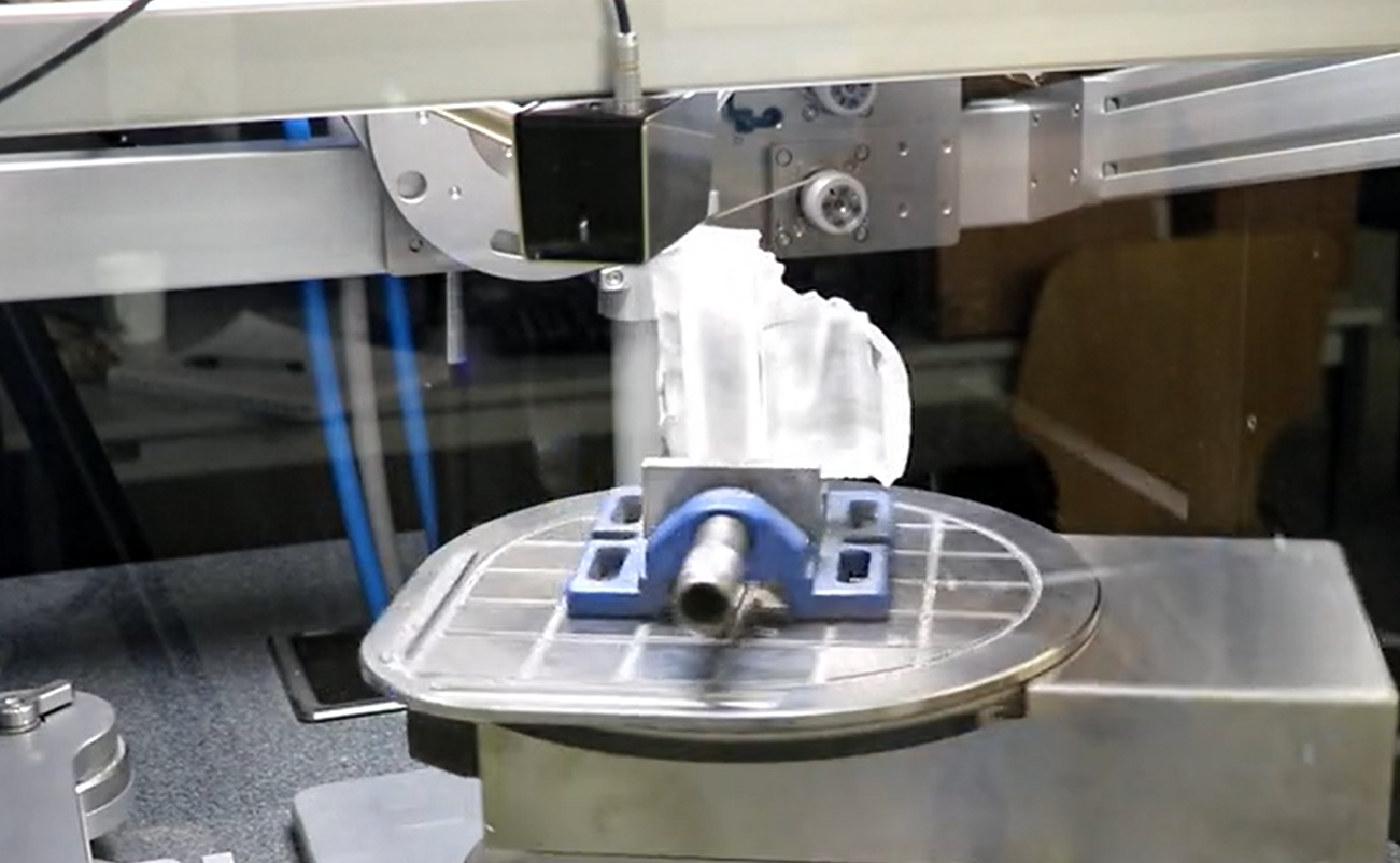
- Large sample compatibility: Supports wafers up to 450 mm in diameter and weights of 30 kg, suitable for materials like silicon carbide (SiC), sapphire, and silicon (Si).
- Modular design: Expandable functionalities include rocking curve analysis, 3D surface defect mapping, and stacking devices for multi-sample processing.
Key Technical Parameters
|
Parameter Category |
Typical Values/Configuration |
|
X-ray Source |
Cu-Kα (0.4×1 mm focal spot), 30 kV accelerating voltage, 0–5 mA adjustable tube current |
|
Angular Range |
θ: -10° to +50°; 2θ: -10° to +100° |
|
Accuracy |
Tilt angle resolution: 0.001°, surface defect detection: ±30 arcseconds (rocking curve) |
|
Scanning Speed |
Omega scan completes full lattice orientation in 5 seconds; Theta scan takes ~1 minute |
|
Sample Stage |
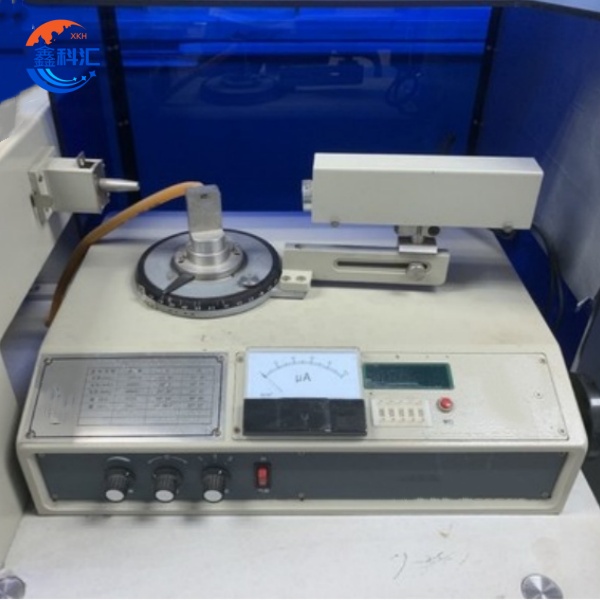
V-groove, pneumatic suction, multi-angle rotation, compatible with 2–8-inch wafers |
|
Expandable Functions |
Rocking curve analysis, 3D mapping, stacking device, optical defect detection (scratches, GBs) |
Working Principle
1. X-ray Diffraction Foundation
- X-rays interact with atomic nuclei and electrons in the crystal lattice, generating diffraction patterns. Bragg’s Law (nλ = 2d sinθ) governs the relationship between diffraction angles (θ) and lattice spacing (d).
Detectors capture these patterns, which are analyzed to reconstruct the crystallographic structure.
2. Omega Scanning Technology
- The crystal rotates continuously around a fixed axis while X-rays illuminate it.
- Detectors collect diffraction signals across multiple crystallographic planes, enabling full lattice orientation determination in 5 seconds.
3. Rocking Curve Analysis
- Fixed crystal angle with varying X-ray incidence angles to measure peak width (FWHM), assessing lattice defects and strain.
4. Automated Control
- PLC and touchscreen interfaces enable preset cutting angles, real-time feedback, and integration with cutting machines for closed-loop control.
Advantages and Features
1. Precision and Efficiency
- Angular accuracy ±0.001°, defect detection resolution <30 arcseconds.
- Omega scan speed is 200× faster than traditional Theta scans.
2. Modularity and Scalability
- Expandable for specialized applications (e.g., SiC wafers, turbine blades).
- Integrates with MES systems for real-time production monitoring.
3. Compatibility and Stability
- Accommodates irregularly shaped samples (e.g., cracked sapphire ingots).
- Air-cooled design reduces maintenance needs.
4. Intelligent Operation
- One-click calibration and multi-task processing.
- Auto-calibration with reference crystals to minimize human error.
Applications
1. Semiconductor Manufacturing
- Wafer dicing orientation: Determines Si, SiC, GaN wafer orientations for optimized cutting efficiency.
- Defect mapping: Identifies surface scratches or dislocations to improve chip yield.
2. Optical Materials
- Nonlinear crystals (e.g., LBO, BBO) for laser devices.
- Sapphire wafer reference surface marking for LED substrates.
3. Ceramics and Composites
- Analyzes grain orientation in Si3N4 and ZrO2 for high-temperature applications.
4. Research and Quality Control
- Universities/labs for novel material development (e.g., high-entropy alloys).
- Industrial QC to ensure batch consistency.
XKH's Services
XKH offers comprehensive lifecycle technical support for wafer orientation instruments, including installation, process parameter optimization, rocking curve analysis, and 3D surface defect mapping. Tailored solutions (e.g., ingot stacking technology) are provided to enhance semiconductor and optical material production efficiency by over 30%. A dedicated team conducts on-site training, while 24/7 remote support and rapid spare part replacement ensure equipment reliability.


