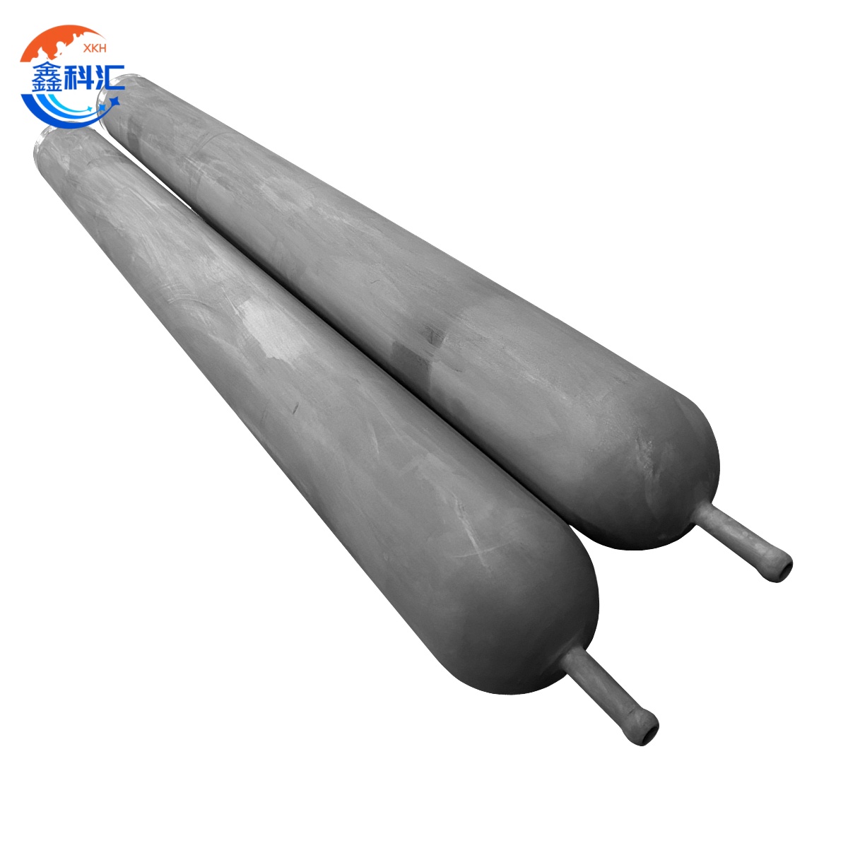
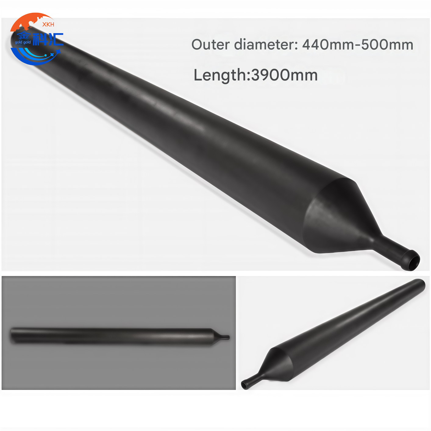
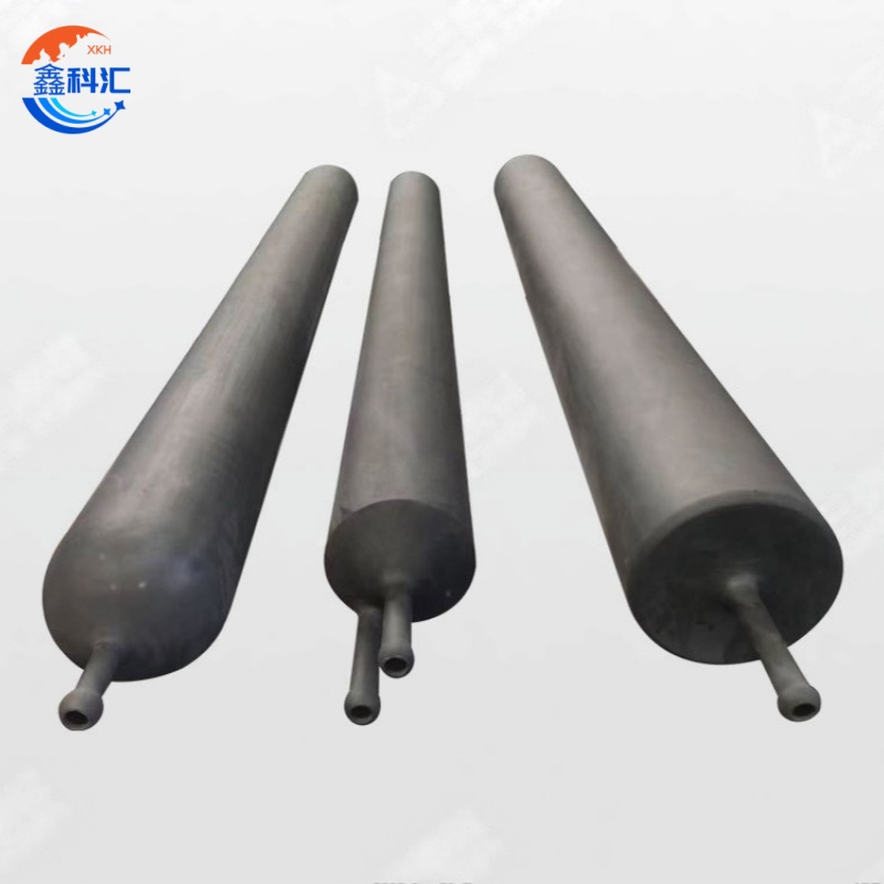
Silicon Carbide (SiC) Horizontal Furnace Tube


Detailed Diagram


Product Positioning & Value Proposition
The Silicon Carbide (SiC) Horizontal Furnace Tube serves as the main process chamber and pressure boundary for high-temperature gas-phase reactions and heat treatments used in semiconductor fabrication, photovoltaic manufacturing, and advanced material processing.
Engineered with a single-piece, additive-manufactured SiC structure combined with a dense CVD-SiC protective layer, this tube delivers exceptional thermal conductivity, minimal contamination, strong mechanical integrity, and outstanding chemical resistance.
Its design ensures superior temperature uniformity, extended service intervals, and stable long-term operation.
Core Advantages
-
Boosts system temperature consistency, cleanliness, and overall equipment effectiveness (OEE).
-
Reduces downtime for cleaning and lengthens replacement cycles, lowering total cost of ownership (TCO).
-
Provides a long-life chamber capable of handling high-temperature oxidative and chlorine-rich chemistries with minimal risk.
Applicable Atmospheres & Process Window
-
Reactive gases: oxygen (O₂) and other oxidizing mixtures
-
Carrier/protective gases: nitrogen (N₂) and ultra-pure inert gases
-
Compatible species: trace chlorine-bearing gases (concentration and dwell time recipe-controlled)
Typical Processes: dry/wet oxidation, annealing, diffusion, LPCVD/CVD deposition, surface activation, photovoltaic passivation, functional thin-film growth, carbonization, nitridation, and more.
Operating Conditions
-
Temperature: room temperature up to 1250 °C (allow 10–15 % safety margin depending on heater design and ΔT)
-
Pressure: from low-pressure/LPCVD vacuum levels to near-atmospheric positive pressure (final spec per purchase order)
Materials & Structural Logic
Monolithic SiC Body (Additive Manufactured)
-
High-density β-SiC or multiphase SiC, built as a single component—no brazed joints or seams that could leak or create stress points.
-
High thermal conductivity enables rapid thermal response and excellent axial/radial temperature uniformity.
-
Low, stable coefficient of thermal expansion (CTE) ensures dimensional stability and reliable seals at elevated temperatures.
 CVD SiC Functional Coating
-
In-situ deposited, ultra-pure (surface/coating impurities < 5 ppm) to suppress particle generation and metal ion release.
-
Superb chemical inertness against oxidizing and chlorine-bearing gases, preventing wall attack or re-deposition.
-
Zone-specific thickness options to balance corrosion resistance and thermal responsiveness.
Combined Benefit: the robust SiC body provides structural strength and heat conduction, while the CVD layer guarantees cleanliness and corrosion resistance for maximum reliability and throughput.
Key Performance Targets
-
Continuous use temperature: ≤ 1250 °C
-
Bulk substrate impurities: < 300 ppm
-
CVD-SiC surface impurities: < 5 ppm
-
Dimensional tolerances: OD ±0.3–0.5 mm; coaxiality ≤ 0.3 mm/m (tighter available)
-
Inner-wall roughness: Ra ≤ 0.8–1.6 µm (polished or near-mirror finish optional)
-
Helium leak rate: ≤ 1 × 10⁻⁹ Pa·m³/s
-
Thermal-shock endurance: survives repeated hot/cold cycling without cracking or spallation
-
Cleanroom assembly: ISO Class 5–6 with certified particle/metal-ion residue levels
Configurations & Options
-
Geometry: OD 50–400 mm (larger by evaluation) with long one-piece construction; wall thickness optimized for mechanical strength, weight, and heat flux.
-
End designs: flanges, bell-mouth, bayonet, locating rings, O-ring grooves, and custom pump-out or pressure ports.
-
Functional ports: thermocouple feedthroughs, sight-glass seats, bypass gas inlets—all engineered for high-temperature, leak-tight operation.
-
Coating schemes: inner wall (default), outer wall, or full coverage; targeted shielding or graded thickness for high-impingement regions.
-
Surface treatment & cleanliness: multiple roughness grades, ultrasonic/DI cleaning, and custom bake/dry protocols.
-
Accessories: graphite/ceramic/metal flanges, seals, locating fixtures, handling sleeves, and storage cradles.
Performance Comparison
| Metric | SiC Tube | Quartz Tube | Alumina Tube | Graphite Tube |
|---|---|---|---|---|
| Thermal conductivity | High, uniform | Low | Low | High |
| High-temp strength/creep | Excellent | Fair | Good | Good (oxidation-sensitive) |
| Thermal shock | Excellent | Weak | Moderate | Excellent |
| Cleanliness / metal ions | Excellent (low) | Moderate | Moderate | Poor |
| Oxidation & Cl-chemistry | Excellent | Fair | Good | Poor (oxidizes) |
| Cost vs. service life | Medium / long life | Low / short | Medium / medium | Medium / environment-limited |
Frequently Asked Questions (FAQ)
Q1. Why choose a 3D-printed monolithic SiC body?
A. It eliminates seams and brazes that can leak or concentrate stress, and supports complex geometries with consistent dimensional accuracy.
Q2. Is SiC resistant to chlorine-bearing gases?
A. Yes. CVD-SiC is highly inert within specified temperature and pressure limits. For high-impact areas, localized thick coatings and robust purge/exhaust systems are recommended.
Q3. How does it outperform quartz tubes?
A. SiC offers longer service life, better temperature uniformity, lower particle/metal-ion contamination, and improved TCO—especially beyond ~900 °C or in oxidizing/chlorinated atmospheres.
Q4. Can the tube handle rapid thermal ramping?
A. Yes, provided maximum ΔT and ramp-rate guidelines are observed. Pairing a high-κ SiC body with a thin CVD layer supports fast thermal transitions.
Q5. When is replacement required?
A. Replace the tube if you detect flange or edge cracks, coating pits or spallation, increasing leak rates, significant temperature-profile drift, or abnormal particle generation.
About Us
XKH specializes in high-tech development, production, and sales of special optical glass and new crystal materials. Our products serve optical electronics, consumer electronics, and the military. We offer Sapphire optical components, mobile phone lens covers, Ceramics, LT, Silicon Carbide SIC, Quartz, and semiconductor crystal wafers. With skilled expertise and cutting-edge equipment, we excel in non-standard product processing, aiming to be a leading optoelectronic materials high-tech enterprise.

Related Products
-

Alumina ceramic arm custom Ceramic robotic arm
-

High-Performance Alumina Ceramic End Effector (...
-

Industrial SiC Vertical Furnace Tube High Therm...
-

Silicon Carbide Ceramic End Effector (Fork Arm/...
-

SiC ceramic chuck tray Ceramic suction cups pre...
-

Silicon Carbide Cantilever Paddle (SiC Cantilev...