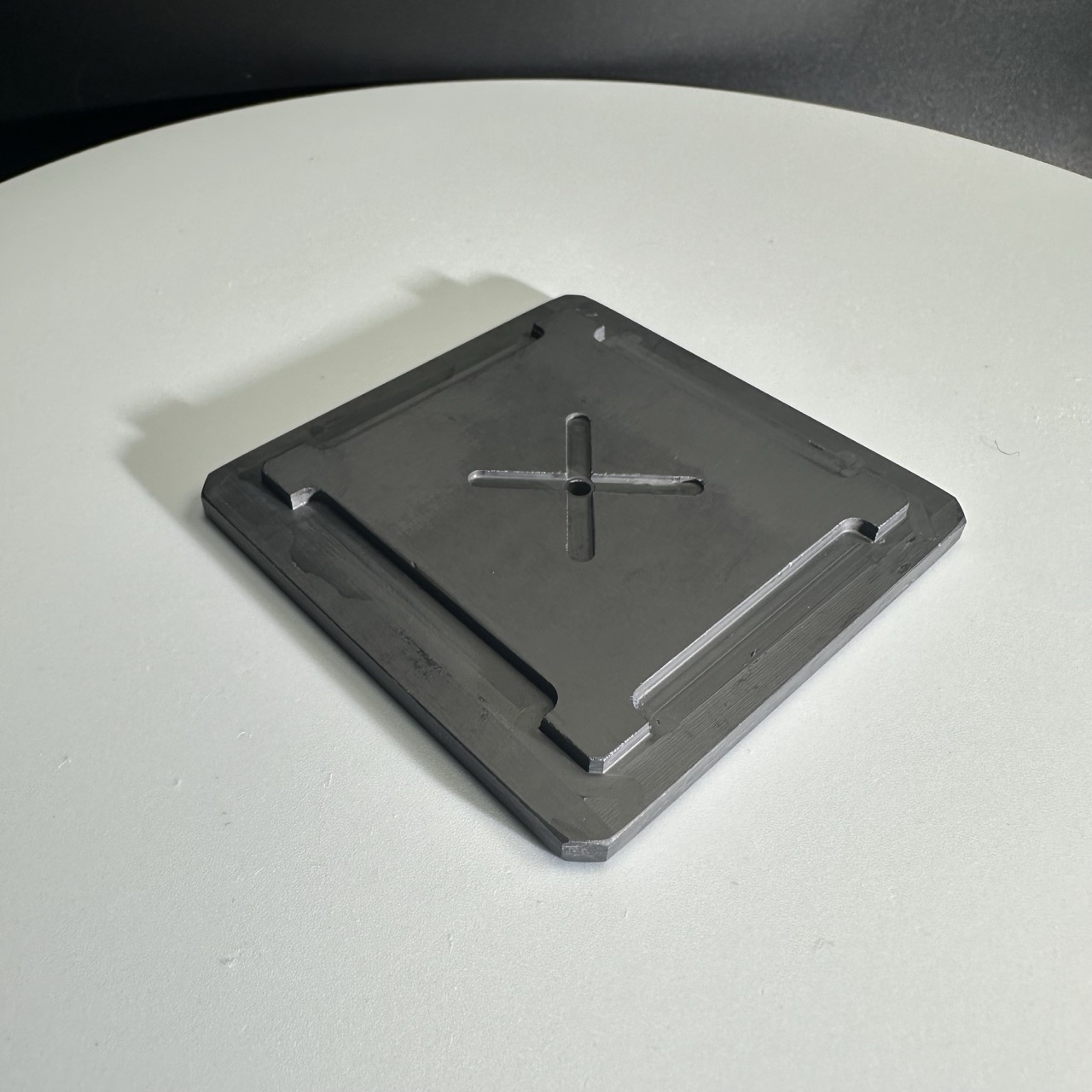
Silicon Carbide Ceramic Chuck for SiC sapphire Si GAAs Wafer


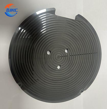
Detailed Diagram
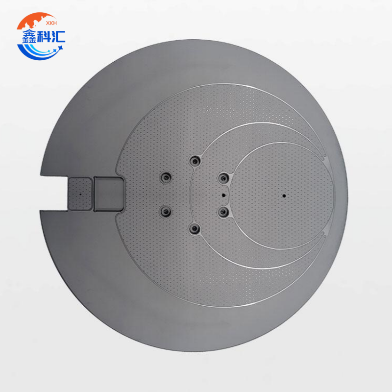
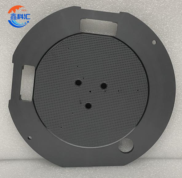
Overview of Silicon Carbide (SiC) Ceramic Chuck
The Silicon Carbide Ceramic Chuck is a high-performance platform engineered for semiconductor inspection, wafer fabrication, and bonding applications. Built with advanced ceramic materials—including sintered SiC (SSiC), reaction-bonded SiC (RSiC), silicon nitride, and aluminum nitride—it offers high stiffness, low thermal expansion, excellent wear resistance, and long service life.
With precision engineering and state-of-the-art polishing, the chuck delivers sub-micron flatness, mirror-quality surfaces, and long-term dimensional stability, making it the ideal solution for critical semiconductor processes.


Key Advantages
-
High Precision
Flatness controlled within 0.3–0.5 μm, ensuring wafer stability and consistent process accuracy. -
Mirror Polishing
Achieves Ra 0.02 μm surface roughness, minimizing wafer scratches and contamination—perfect for ultra-clean environments. -
Ultra-Lightweight
Stronger yet lighter than quartz or metal substrates, improving motion control, responsiveness, and positioning accuracy. -
High Stiffness
Exceptional Young’s modulus ensures dimensional stability under heavy loads and high-speed operation. -
Low Thermal Expansion
CTE closely matches silicon wafers, reducing thermal stress and enhancing process reliability. -
Outstanding Wear Resistance
Extreme hardness preserves flatness and precision even under long-term, high-frequency use.
Manufacturing Process
-
Raw Material Preparation
High-purity SiC powders with controlled particle size and ultra-low impurities. -
Forming & Sintering
Techniques such as pressureless sintering (SSiC) or reaction bonding (RSiC) produce dense, uniform ceramic substrates. -
Precision Machining
CNC grinding, laser trimming, and ultra-precision machining achieve ±0.01 mm tolerance and ≤3 μm parallelism. -
Surface Treatment
Multi-stage grinding and polishing to Ra 0.02 μm; optional coatings available for corrosion resistance or customized friction properties. -
Inspection & Quality Control
Interferometers and roughness testers verify compliance with semiconductor-grade specifications.
Technical Specifications
| Parameter | Value | Unit |
|---|---|---|
| Flatness | ≤0.5 | μm |
| Wafer sizes | 6’’, 8’’, 12’’ (custom available) | — |
| Surface type | Pin type / Ring type | — |
| Pin height | 0.05–0.2 | mm |
| Min. pin diameter | ϕ0.2 | mm |
| Min. pin spacing | 3 | mm |
| Min. seal ring width | 0.7 | mm |
| Surface roughness | Ra 0.02 | μm |
| Thickness tolerance | ±0.01 | mm |
| Diameter tolerance | ±0.01 | mm |
| Parallelism tolerance | ≤3 | μm |
Main Applications
-
Semiconductor wafer inspection equipment
-
Wafer fabrication and transfer systems
-
Wafer bonding & packaging tools
-
Advanced optoelectronic device manufacturing
-
Precision instruments requiring ultra-flat, ultra-clean surfaces
Q&A – Silicon Carbide Ceramic Chuck
Q1: How do SiC ceramic chucks compare with quartz or metal chucks?
A1: SiC chucks are lighter, stiffer, and have a CTE close to silicon wafers, minimizing thermal deformation. They also offer superior wear resistance and longer lifetime.
Q2: What flatness can be achieved?
A2: Controlled within 0.3–0.5 μm, meeting the stringent demands of semiconductor production.
Q3: Will the surface scratch wafers?
A3: No—mirror-polished to Ra 0.02 μm, ensuring scratch-free handling and reduced particle generation.
Q4: What wafer sizes are supported?
A4: Standard sizes of 6’’, 8’’, and 12’’, with customization available.
Q5: How is the thermal resistance?
A5: SiC ceramics provide excellent high-temperature performance with minimal deformation under thermal cycling.
About Us
XKH specializes in high-tech development, production, and sales of special optical glass and new crystal materials. Our products serve optical electronics, consumer electronics, and the military. We offer Sapphire optical components, mobile phone lens covers, Ceramics, LT, Silicon Carbide SIC, Quartz, and semiconductor crystal wafers. With skilled expertise and cutting-edge equipment, we excel in non-standard product processing, aiming to be a leading optoelectronic materials high-tech enterprise.

Related Products
-

Silicon Carbide Ceramic End Effector (Fork Arm/...
-
Dia3mm SiC Ceramic ball Silicon carbide Ceramic...
-
Custom industrial SiC ceramic parts factory res...
-

Silicon Carbide Prism / Mirror For Infrared Opt...
-

Alumina ceramic arm custom Ceramic robotic arm
-

SiC Ceramic Fork Arm / End Effector – Advanced ...