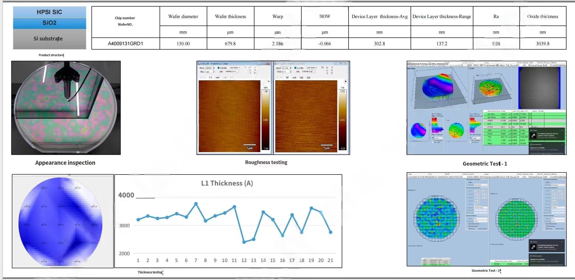
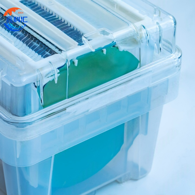
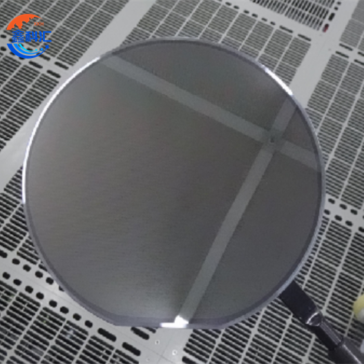
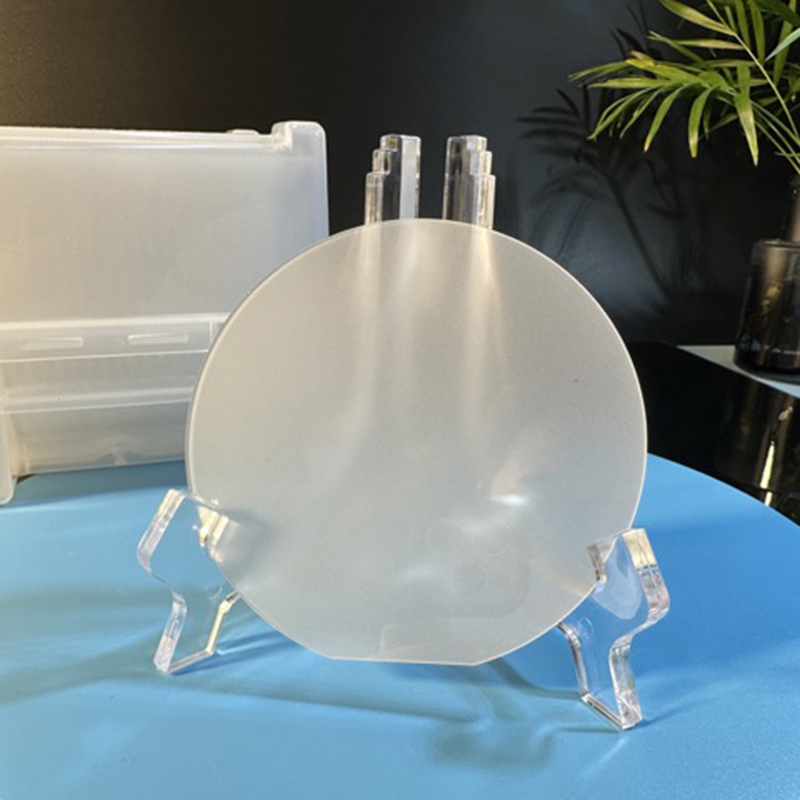
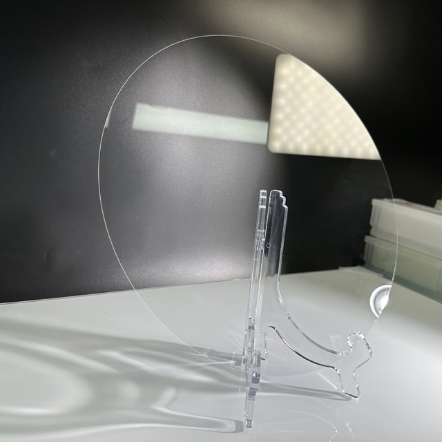
SiCOI wafer 4inch 6inch HPSI SiC SiO2 Si subatrate structure


SiCOI wafer‘s structure
HPB (High-Performance Bonding) BIC (Bonded Integrated Circuit) and SOD (Silicon-on-Diamond or Silicon-on-Insulator-like technology). It includes:
Performance Metrics:
Lists parameters like accuracy, error types (e.g., "No error," "Value distance"), and thickness measurements (e.g., "Direct-Layer thickness/kg").
A table with numerical values (possibly experimental or process parameters) under headings like "ADDR/SYGBDT," "10/0," etc.
Layer Thickness Data:
Extensive repetitive entries labeled "L1 Thickness (A)" to "L270 Thickness (A)" (likely in Ångströms, 1 Å = 0.1 nm).
Suggests a multi-layered structure with precise thickness control for each layer, typical in advanced semiconductor wafers.
SiCOI Wafer Structure
SiCOI (Silicon Carbide on Insulator) is a specialized wafer structure combining silicon carbide (SiC) with an insulating layer, similar to SOI (Silicon-on-Insulator) but optimized for high-power/high-temperature applications. Key features:
Layer Composition:
Top Layer: Single-crystal Silicon Carbide (SiC) for high electron mobility and thermal stability.
Buried Insulator: Typically SiO₂ (oxide) or diamond (in SOD) to reduce parasitic capacitance and improve isolation.
Base Substrate: Silicon or polycrystalline SiC for mechanical support
SiCOI wafer‘s properties
Electrical Properties Wide Bandgap (3.2 eV for 4H-SiC):Enables high breakdown voltage (>10× higher than silicon).Reduces leakage currents, improving efficiency in power devices.
High Electron Mobility:~900 cm²/V·s (4H-SiC) vs. ~1,400 cm²/V·s (Si), but better high-field performance.
Low On-Resistance:SiCOI-based transistors (e.g., MOSFETs) exhibit lower conduction losses.
Excellent Insulation:The buried oxide (SiO₂) or diamond layer minimizes parasitic capacitance and crosstalk.
- Thermal PropertiesHigh Thermal Conductivity:SiC (~490 W/m·K for 4H-SiC) vs. Si (~150 W/m·K).Diamond (if used as insulator) can exceed 2,000 W/m·K, enhancing heat dissipation.
Thermal Stability:Operates reliably at >300°C (vs. ~150°C for silicon).Reduces cooling requirements in power electronics.
3. Mechanical & Chemical PropertiesExtreme Hardness (~9.5 Mohs):Resists wear, making SiCOI durable for harsh environments.
Chemical Inertness:Resists oxidation and corrosion, even in acidic/alkaline conditions.
Low Thermal Expansion:Matches well with other high-temperature materials (e.g., GaN).
4. Structural Advantages (vs. Bulk SiC or SOI)
Reduced Substrate Losses:Insulating layer prevents current leakage into the substrate.
Improved RF Performance:Lower parasitic capacitance enables faster switching (useful for 5G/mmWave devices).
Flexible Design:Thin SiC top layer allows for optimized device scaling (e.g., ultra-thin channels in transistors).
Comparison with SOI & Bulk SiC
| Property | SiCOI | SOI (Si/SiO₂/Si) | Bulk SiC |
| Bandgap | 3.2 eV (SiC) | 1.1 eV (Si) | 3.2 eV (SiC) |
| Thermal Conductivity | High (SiC + diamond) | Low (SiO₂ limits heat flow) | High (SiC only) |
| Breakdown Voltage | Very High | Moderate | Very High |
| Cost | Higher | Lower | Highest (pure SiC) |
SiCOI wafer‘s applications
Power Electronics
SiCOI wafers are widely used in high-voltage and high-power semiconductor devices such as MOSFETs, Schottky diodes, and power switches. The wide bandgap and high breakdown voltage of SiC enable efficient power conversion with reduced losses and enhanced thermal performance.
Radio Frequency (RF) Devices
The insulating layer in SiCOI wafers reduces parasitic capacitance, making them suitable for high-frequency transistors and amplifiers used in telecommunications, radar, and 5G technologies.
Microelectromechanical Systems (MEMS)
SiCOI wafers provide a robust platform for fabricating MEMS sensors and actuators that operate reliably in harsh environments due to SiC’s chemical inertness and mechanical strength.
High-Temperature Electronics
SiCOI enables electronics that maintain performance and reliability at elevated temperatures, benefiting automotive, aerospace, and industrial applications where conventional silicon devices fail.
Photonic and Optoelectronic Devices
The combination of SiC’s optical properties and the insulating layer facilitates integration of photonic circuits with enhanced thermal management.
Radiation-Hardened Electronics
Due to the inherent radiation tolerance of SiC, SiCOI wafers are ideal for space and nuclear applications requiring devices that withstand high-radiation environments.
SiCOI wafer‘s Q&A
Q1: What is a SiCOI wafer?
A: SiCOI stands for Silicon Carbide-on-Insulator. It is a semiconductor wafer structure where a thin layer of silicon carbide (SiC) is bonded onto an insulating layer (usually silicon dioxide, SiO₂), which is supported by a silicon substrate. This structure combines SiC’s excellent properties with electrical isolation from the insulator.
Q2: What are the main advantages of SiCOI wafers?
A: The main advantages include high breakdown voltage, wide bandgap, excellent thermal conductivity, superior mechanical hardness, and reduced parasitic capacitance thanks to the insulating layer. This leads to improved device performance, efficiency, and reliability.
Q3: What are typical applications of SiCOI wafers?
A: They are used in power electronics, high-frequency RF devices, MEMS sensors, high-temperature electronics, photonic devices, and radiation-hardened electronics.
Detailed Diagram
Related Products
-

6 in Silicon Carbide 4H-SiC Semi-Insulating Ing...
-

sapphire ball lens optical grade Al2O3 material...
-
2 inch 50.8mm Thickness 0.1mm 0.2mm 0.43mm Sapp...
-
12 inch Dia300x1.0mmt Sapphire Wafer Substrate ...
-

SOI wafer insulator on silicon 8-inch and 6-inc...
-

Single Crystal Silicon Wafer Si Substrate Type ...