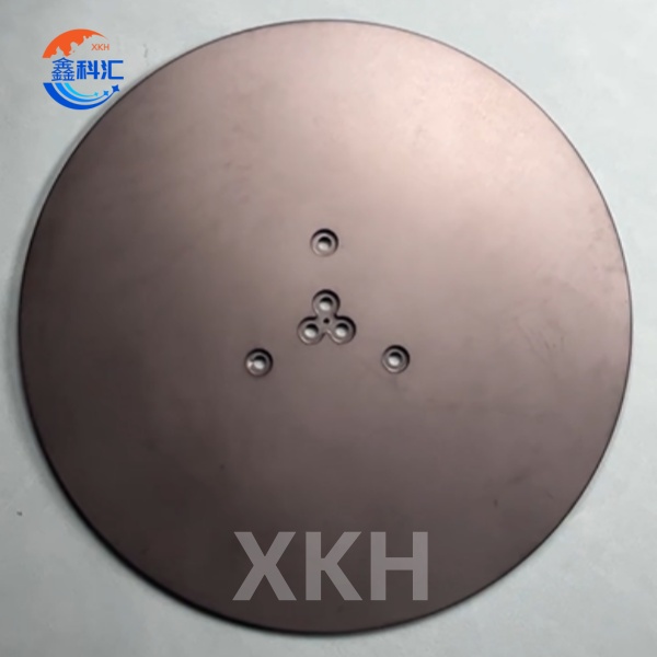
SiC Ceramic Tray for Wafer Carrier with High-Temperature Resistance


Silicon Carbide Ceramic Tray (SiC Tray)
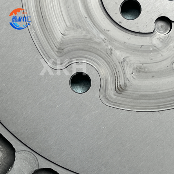
A high-performance ceramic component based on silicon carbide (SiC) material, engineered for advanced industrial applications such as semiconductor manufacturing and LED production. Its core functions include serving as a wafer carrier, etching process platform, or high-temperature process support, leveraging exceptional thermal conductivity, high-temperature resistance, and chemical stability to ensure process uniformity and product yield.
Key Features
1. Thermal Performance
- High Thermal Conductivity: 140–300 W/m·K, significantly surpassing traditional graphite (85 W/m·K), enabling rapid heat dissipation and reduced thermal stress.
- Low Thermal Expansion Coefficient: 4.0×10⁻⁶/℃ (25–1000℃), closely matching silicon (2.6×10⁻⁶/℃), minimizing thermal deformation risks.
2. Mechanical Properties
- High Strength: Flexural strength ≥320 MPa (20℃), resistant to compression and impact.
- High Hardness: Mohs hardness 9.5, second only to diamond, offering superior wear resistance.
3. Chemical Stability
- Corrosion Resistance: Resistant to strong acids (e.g., HF, H₂SO₄), suitable for etching process environments.
- Non-Magnetic: Intrinsic magnetic susceptibility <1×10⁻⁶ emu/g, avoiding interference with precision instruments.
4. Extreme Environment Tolerance
- High-Temperature Durability: Long-term operational temperature up to 1600–1900℃; short-term resistance up to 2200℃ (oxygen-free environment).
- Thermal Shock Resistance: Withstands abrupt temperature changes (ΔT >1000℃) without cracking.
Applications
|
Application Field |
Specific Scenarios |
Technical Value |
|
Semiconductor Manufacturing |
Wafer etching (ICP), thin-film deposition (MOCVD), CMP polishing |
High thermal conductivity ensures uniform temperature fields; low thermal expansion minimizes wafer warpage. |
|
LED Production |
Epitaxial growth (e.g., GaN), wafer dicing, packaging |
Suppresses multi-type defects, enhancing LED luminous efficiency and lifespan. |
|
Photovoltaic Industry |
Silicon wafer sintering furnaces, PECVD equipment supports |
High-temperature and thermal shock resistance extend equipment lifespan. |
|
Laser & Optics |
High-power laser cooling substrates, optical system supports |
High thermal conductivity enables rapid heat dissipation, stabilizing optical components. |
|
Analytical Instruments |
TGA/DSC sample holders |
Low heat capacity and fast thermal response improve measurement accuracy. |
Produc Advantages
- Comprehensive Performance: Thermal conductivity, strength, and corrosion resistance far exceed alumina and silicon nitride ceramics, meeting extreme operational demands.
- Lightweight Design: Density of 3.1–3.2 g/cm³ (40% of steel), reducing inertial load and enhancing motion precision.
- Longevity & Reliability: Service life exceeds 5 years at 1600℃, reducing downtime and lowering operational costs by 30%.
- Customization: Supports complex geometries (e.g., porous suction cups, multi-layer trays) with flatness error <15 μm for precision applications.
Technical Specifications
|
Parameter Category |
Indicator |
|
Physical Properties |
|
|
Density |
≥3.10 g/cm³ |
|
Flexural Strength (20℃) |
320–410 MPa |
|
Thermal Conductivity (20℃) |
140–300 W/(m·K) |
|
Thermal Expansion Coefficient (25–1000℃) |
4.0×10⁻⁶/℃ |
|
Chemical Properties |
|
|
Acid Resistance (HF/H₂SO₄) |
No corrosion after 24h immersion |
|
Machining Precision |
|
|
Flatness |
≤15 μm (300×300 mm) |
|
Surface Roughness (Ra) |
≤0.4 μm |
XKH's Services
XKH provides comprehensive industrial solutions spanning custom development, precision machining, and rigorous quality control. For custom development, it offers high-purity (>99.999%) and porous (30–50% porosity) material solutions, paired with 3D modeling and simulation to optimize complex geometries for applications like semiconductors and aerospace. Precision machining follows a streamlined process: powder processing → isostatic/dry pressing → 2200°C sintering → CNC/diamond grinding → inspection, ensuring nanometer-level polishing and ±0.01 mm dimensional tolerance. Quality control includes full-process testing (XRD composition, SEM microstructure, 3-point bending) and technical support (process optimization, 24/7 consultation, 48-hour sample delivery), delivering reliable, high-performance components for advanced industrial needs.
Frequently Asked Questions (FAQ)
1. Q: What industries use silicon carbide ceramic trays?
A: Widely used in semiconductor manufacturing (wafer handling), solar energy (PECVD processes), medical equipment (MRI components), and aerospace (high-temperature parts) due to their extreme heat resistance and chemical stability.
2. Q: How does silicon carbide outperform quartz/glass trays?
A: Higher thermal shock resistance (up to 1800°C vs. quartz’s 1100°C), zero magnetic interference, and longer lifespan (5+ years vs. quartz’s 6-12 months).
3. Q: Can silicon carbide trays handle acidic environments?
A: Yes. Resistant to HF, H2SO4, and NaOH with <0.01mm corrosion/year, making them ideal for chemical etching and wafer cleaning.
4. Q: Are silicon carbide trays compatible with automation?
A: Yes. Designed for vacuum pickup and robotic handling, with surface flatness <0.01mm to prevent particle contamination in automated fabs.
5. Q: What’s the cost comparison vs. traditional materials?
A: Higher upfront cost (3-5x quartz) but 30-50% lower TCO due to extended lifespan, reduced downtime, and energy savings from superior thermal conductivity.


