-
Why semi-insulating SiC over conductive SiC?
Semi-insulating SiC offers much higher resistivity, which reduces leakage currents in high-voltage and high-frequency devices. Conductive SiC is more suitable for applications where electrical conductivity is needed. -
Can these wafers be used for epitaxial growth?
Yes, these wafers are epi-ready and optimized for MOCVD, HVPE, or MBE, with surface treatments and defect control to ensure superior epitaxial layer quality. -
How do you ensure wafer cleanliness?
A Class-100 cleanroom process, multi-step ultrasonic cleaning, and nitrogen-sealed packaging guarantee that the wafers are free from contaminants, residues, and micro-scratches. -
What is the lead time for orders?
Samples typically ship within 7–10 business days, while production orders are usually delivered in 4–6 weeks, depending on the specific wafer size and custom features. -
Can you provide custom shapes?
Yes, we can create custom substrates in various shapes such as planar windows, V-grooves, spherical lenses, and more.
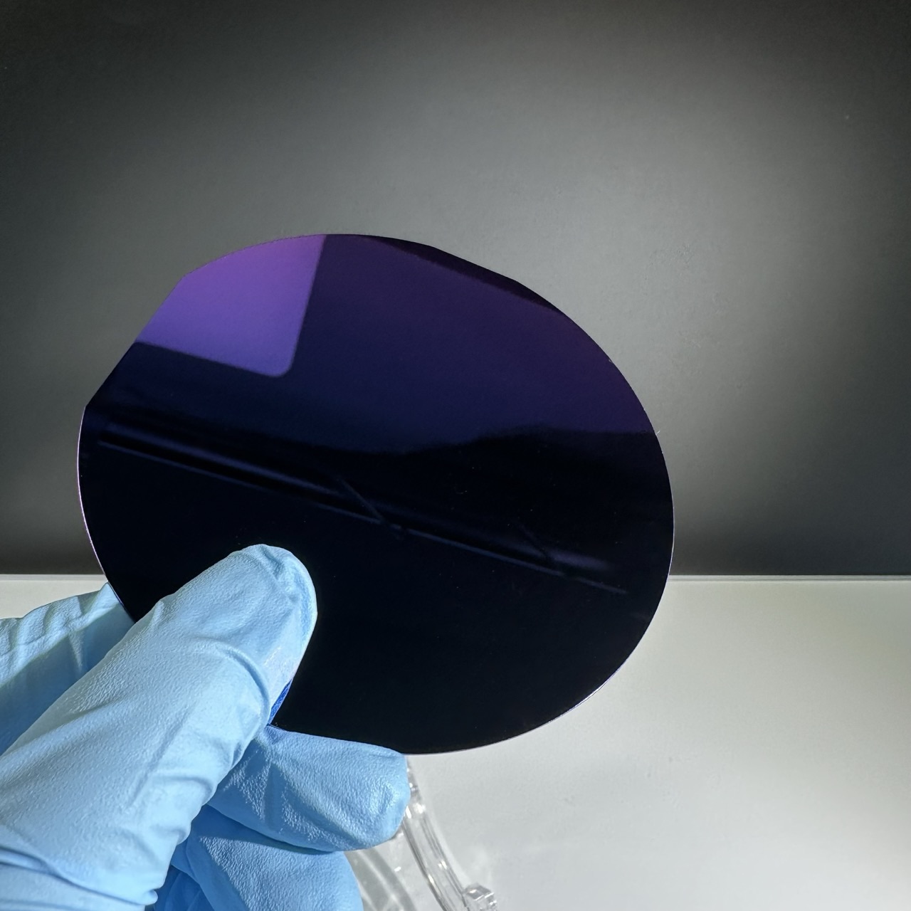
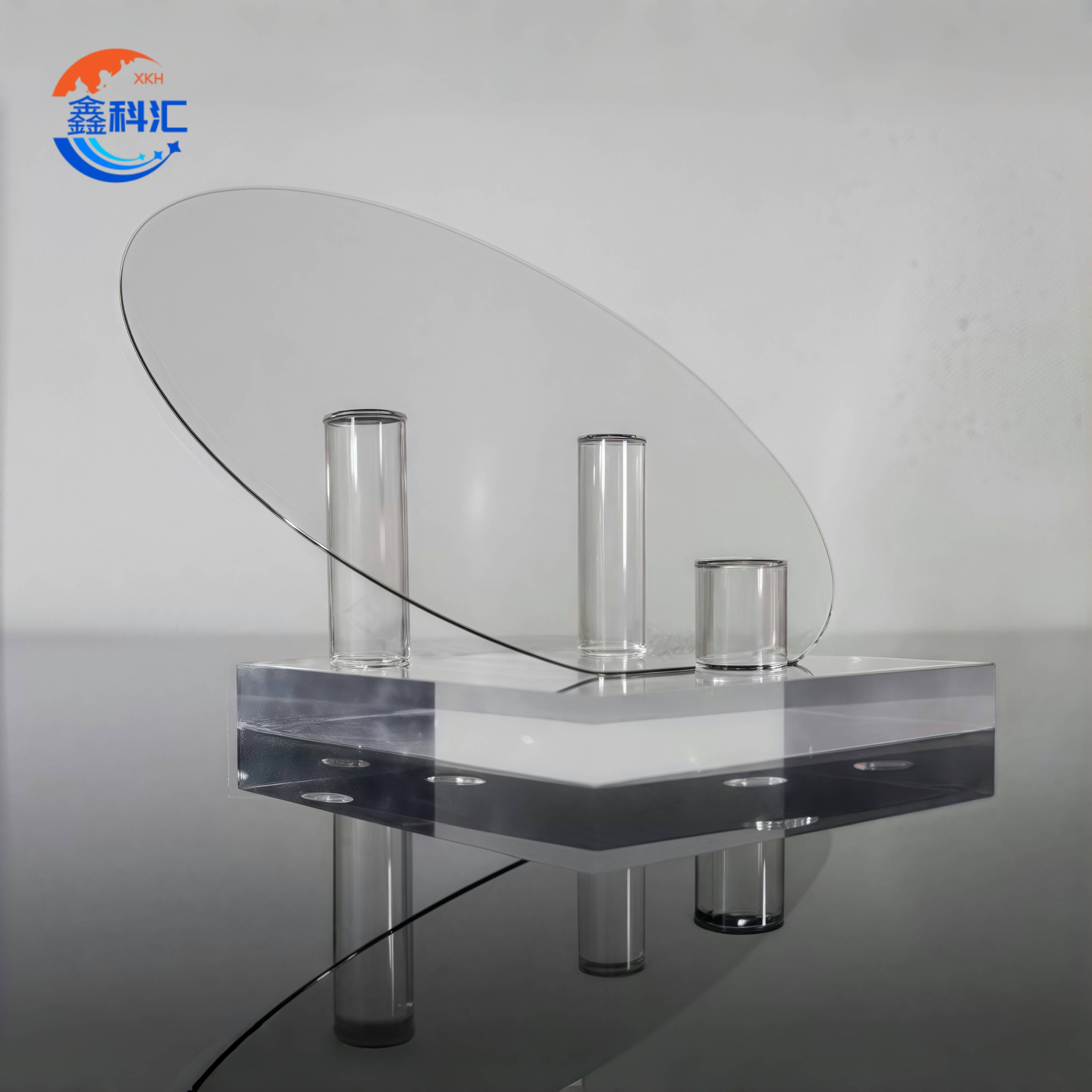
Semi-Insulating Silicon Carbide (SiC) Substrate High-Purity For Ar Glasses

Detailed Diagram
Product Overview of Semi-Insulating SiC Wafers
ur High-Purity Semi-Insulating SiC Wafers are designed for advanced power electronics, RF/microwave components, and optoelectronic applications. These wafers are manufactured from high-quality 4H- or 6H-SiC single crystals, using a refined Physical Vapor Transport (PVT) growth method, followed by deep-level compensation annealing. The outcome is a wafer with the following outstanding properties:
-
Ultra-High Resistivity: ≥1×10¹² Ω·cm, effectively minimizing leakage currents in high-voltage switching devices.
-
Wide Bandgap (~3.2 eV): Ensures excellent performance in high-temperature, high-field, and radiation-intensive environments.
-
Exceptional Thermal Conductivity: >4.9 W/cm·K, providing efficient heat dissipation in high-power applications.
-
Superior Mechanical Strength: With a Mohs hardness of 9.0 (second only to diamond), low thermal expansion, and strong chemical stability.
-
Atomically Smooth Surface: Ra < 0.4 nm and defect density < 1/cm², ideal for MOCVD/HVPE epitaxy and micro-nano fabrication.
Available Sizes: Standard sizes include 50, 75, 100, 150, and 200 mm (2"–8"), with custom diameters available up to 250 mm.
Thickness Range: 200–1,000 μm, with a tolerance of ±5 μm.


Manufacturing Process of Semi-Insulating SiC Wafers
High-Purity SiC Powder Preparation
-
Starting Material: 6N-grade SiC powder, purified using multi-stage vacuum sublimation and thermal treatments, ensuring low metal contamination (Fe, Cr, Ni < 10 ppb) and minimal polycrystalline inclusions.
Modified PVT Single-Crystal Growth
-
Environment: Near-vacuum (10⁻³–10⁻² Torr).
-
Temperature: Graphite crucible heated to ~2,500 °C with a controlled thermal gradient of ΔT ≈ 10–20 °C/cm.
-
Gas Flow & Crucible Design: Tailored crucible and porous separators ensure uniform vapor distribution and suppress unwanted nucleation.
-
Dynamic Feed & Rotation: Periodic replenishment of SiC powder and crystal-rod rotation results in low dislocation densities (<3,000 cm⁻²) and consistent 4H/6H orientation.
Deep-Level Compensation Annealing
-
Hydrogen Anneal: Conducted in H₂ atmosphere at temperatures between 600–1,400 °C to activate deep-level traps and stabilize intrinsic carriers.
-
N/Al Co-Doping (Optional): Incorporation of Al (acceptor) and N (donor) during growth or post-growth CVD to form stable donor-acceptor pairs, driving resistivity peaks.
Precision Slicing & Multi-Stage Lapping
-
Diamond-Wire Sawing: Wafers sliced to a thickness of 200–1,000 μm, with minimal damage and a tolerance of ±5 μm.
-
Lapping Process: Sequential coarse-to-fine diamond abrasives remove saw damage, preparing the wafer for polishing.
Chemical Mechanical Polishing (CMP)
-
Polishing Media: Nano-oxide (SiO₂ or CeO₂) slurry in mild alkaline solution.
-
Process Control: Low-stress polishing minimizes roughness, achieving RMS roughness of 0.2–0.4 nm and eliminating micro-scratches.
Final Cleaning & Packaging
-
Ultrasonic Cleaning: Multi-step cleaning process (organic solvent, acid/base treatments, and deionized water rinse) in a Class-100 cleanroom environment.
-
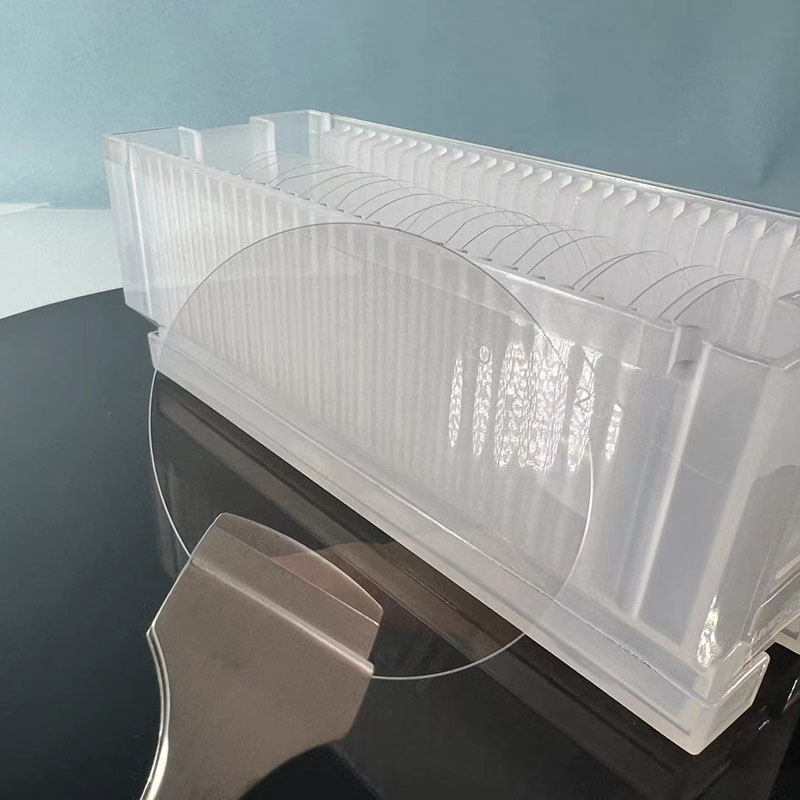
Sealing & Packaging: Wafer drying with nitrogen purge, sealed in nitrogen-filled protective bags and packed in anti-static, vibration-dampening outer boxes.
Specifications of Semi-Insulating SiC Wafers
| Product Performance | Grade P | Grade D |
|---|---|---|
| I. Crystal Parameters | I. Crystal Parameters | I. Crystal Parameters |
| Crystal Polytype | 4H | 4H |
| Refractive Index a | >2.6 @589nm | >2.6 @589nm |
| Absorption Rate a | ≤0.5% @450-650nm | ≤1.5% @450-650nm |
| MP Transmittance a (Uncoated) | ≥66.5% | ≥66.2% |
| Haze a | ≤0.3% | ≤1.5% |
| Polytype Inclusion a | Not allowed | Cumulative area ≤20% |
| Micropipe Density a | ≤0.5 /cm² | ≤2 /cm² |
| Hexagonal Void a | Not allowed | N/A |
| Faceted Inclusion a | Not allowed | N/A |
| MP Inclusion a | Not allowed | N/A |
| II. Mechanical Parameters | II. Mechanical Parameters | II. Mechanical Parameters |
| Diameter | 150.0 mm +0.0 mm / -0.2 mm | 150.0 mm +0.0 mm / -0.2 mm |
| Surface Orientation | {0001} ±0.3° | {0001} ±0.3° |
| Primary Flat Length | Notch | Notch |
| Secondary Flat Length | No secondary flat | No secondary flat |
| Notch Orientation | <1-100> ±2° | <1-100> ±2° |
| Notch Angle | 90° +5° / -1° | 90° +5° / -1° |
| Notch Depth | 1 mm from edge +0.25 mm / -0.0 mm | 1 mm from edge +0.25 mm / -0.0 mm |
| Surface Treatment | C-face, Si-face: Chemo-Mechanical Polishing (CMP) | C-face, Si-face: Chemo-Mechanical Polishing (CMP) |
| Wafer Edge | Chamfered (Rounded) | Chamfered (Rounded) |
| Surface Roughness (AFM) (5μm x 5μm) | Si-face, C-face: Ra ≤ 0.2 nm | Si-face, C-face: Ra ≤ 0.2 nm |
| Thickness a (Tropel) | 500.0 μm ± 25.0 μm | 500.0 μm ± 25.0 μm |
| LTV (Tropel) (40mm x 40mm) a | ≤ 2 μm | ≤ 4 μm |
| Total Thickness Variation (TTV) a (Tropel) | ≤ 3 μm | ≤ 5 μm |
| Bow (Absolute Value) a (Tropel) | ≤ 5 μm | ≤ 15 μm |
| Warp a (Tropel) | ≤ 15 μm | ≤ 30 μm |
| III. Surface Parameters | III. Surface Parameters | III. Surface Parameters |
| Chip/Notch | Not allowed | ≤ 2 pcs, each length and width ≤ 1.0 mm |
| Scratch a (Si-face, CS8520) | Total length ≤ 1 x Diameter | Total length ≤ 3 x Diameter |
| Particle a (Si-face, CS8520) | ≤ 500 pcs | N/A |
| Crack | Not allowed | Not allowed |
| Contamination a | Not allowed | Not allowed |
Key Applications of Semi-Insulating SiC Wafers
-
High-Power Electronics: SiC-based MOSFETs, Schottky diodes, and power modules for electric vehicles (EVs) benefit from SiC’s low on-resistance and high-voltage capabilities.
-
RF & Microwave: SiC’s high-frequency performance and radiation resistance are ideal for 5G base-station amplifiers, radar modules, and satellite communications.
-
Optoelectronics: UV-LEDs, blue-laser diodes, and photodetectors utilize atomically smooth SiC substrates for uniform epitaxial growth.
-
Extreme Environment Sensing: SiC’s stability at high temperatures (>600 °C) makes it perfect for sensors in harsh environments, including gas turbines and nuclear detectors.
-
Aerospace & Defense: SiC offers durability for power electronics in satellites, missile systems, and aviation electronics.
-
Advanced Research: Custom solutions for quantum computing, micro-optics, and other specialized research applications.
FAQs
About Us
XKH specializes in high-tech development, production, and sales of special optical glass and new crystal materials. Our products serve optical electronics, consumer electronics, and the military. We offer Sapphire optical components, mobile phone lens covers, Ceramics, LT, Silicon Carbide SIC, Quartz, and semiconductor crystal wafers. With skilled expertise and cutting-edge equipment, we excel in non-standard product processing, aiming to be a leading optoelectronic materials high-tech enterprise.