Sapphire Tube EFG Ky Method Optical Grade Al2O3 Crystal


Detailed Diagram


Product Overview
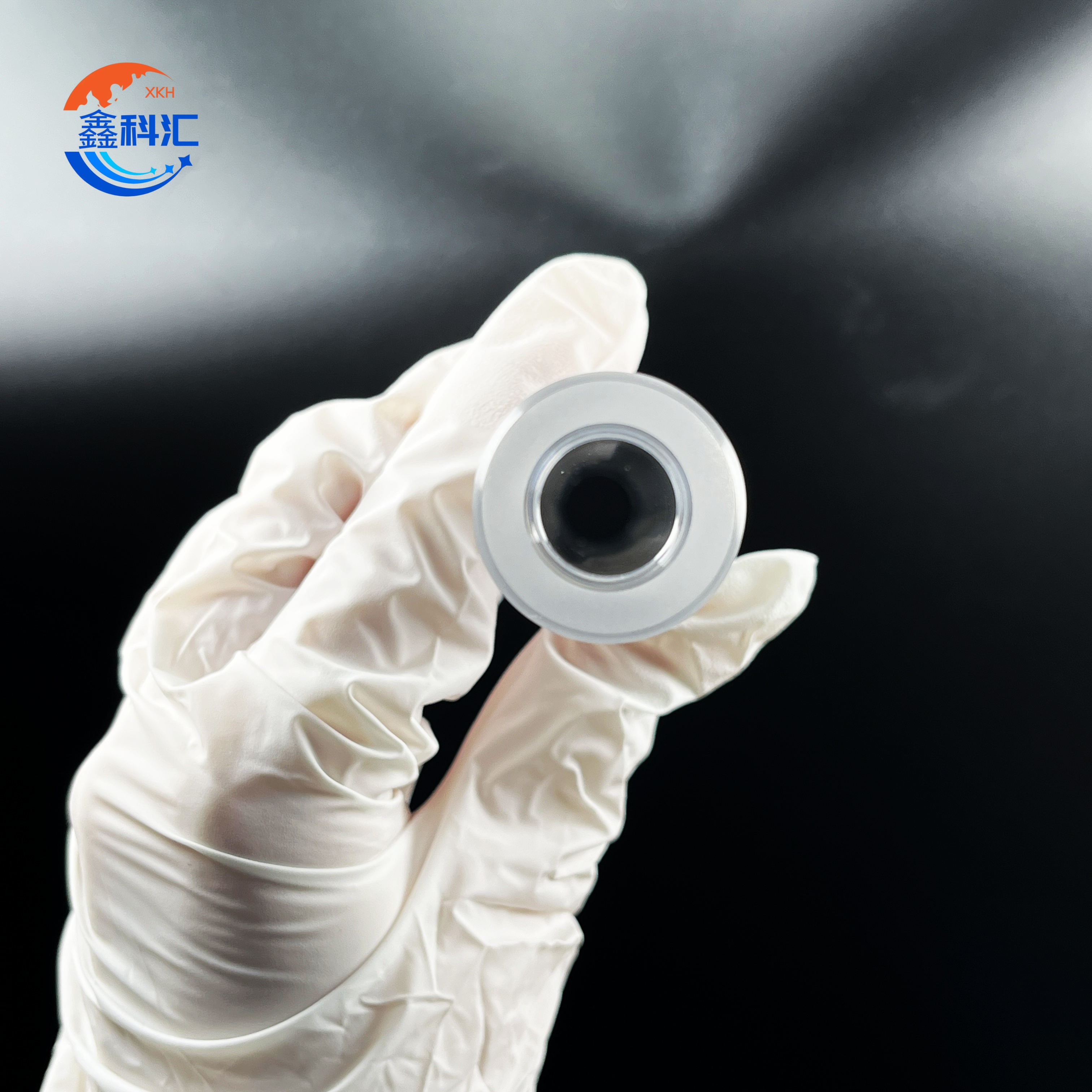
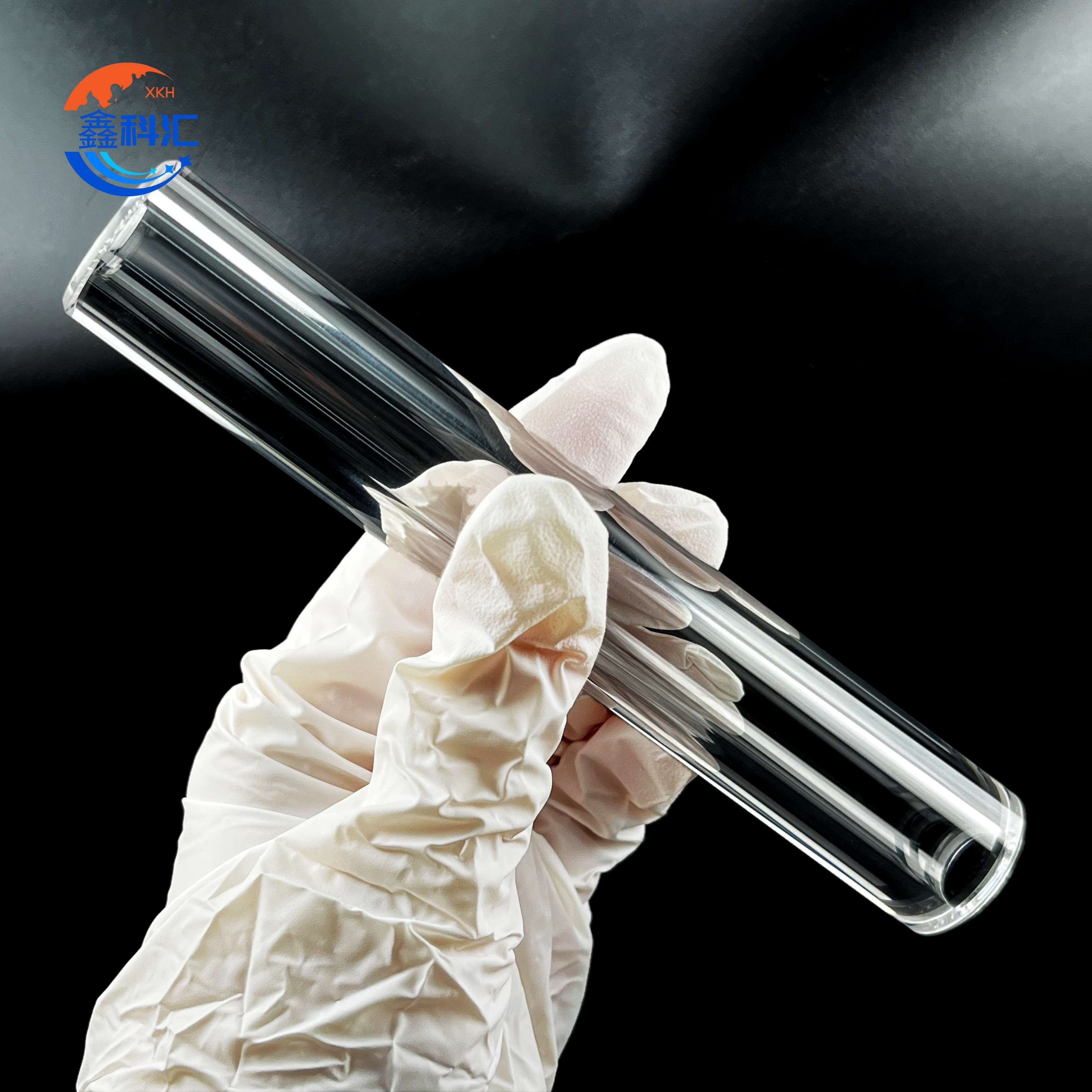
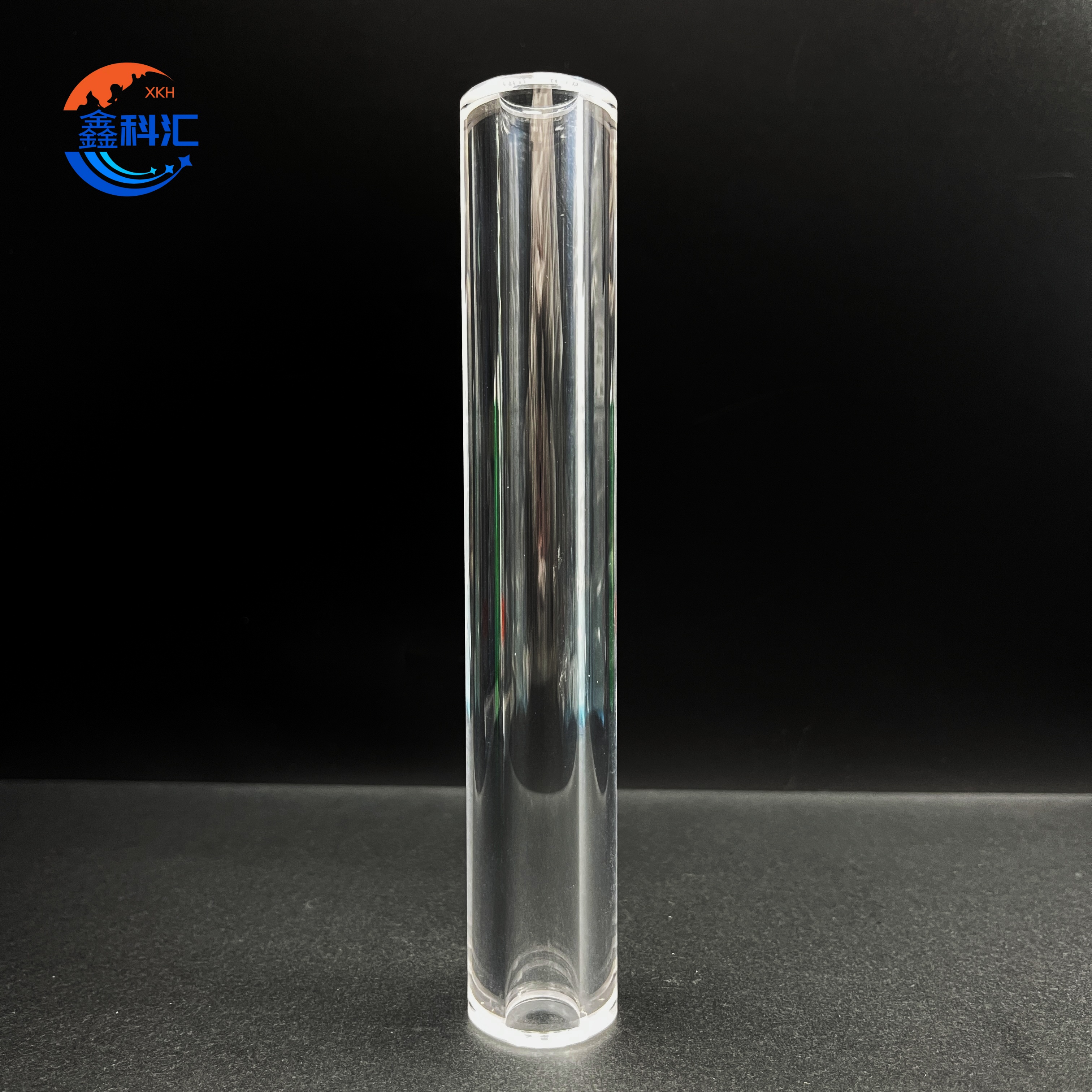
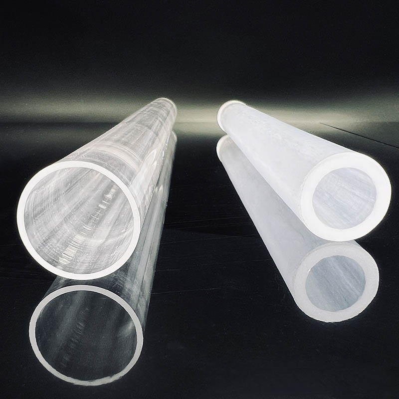
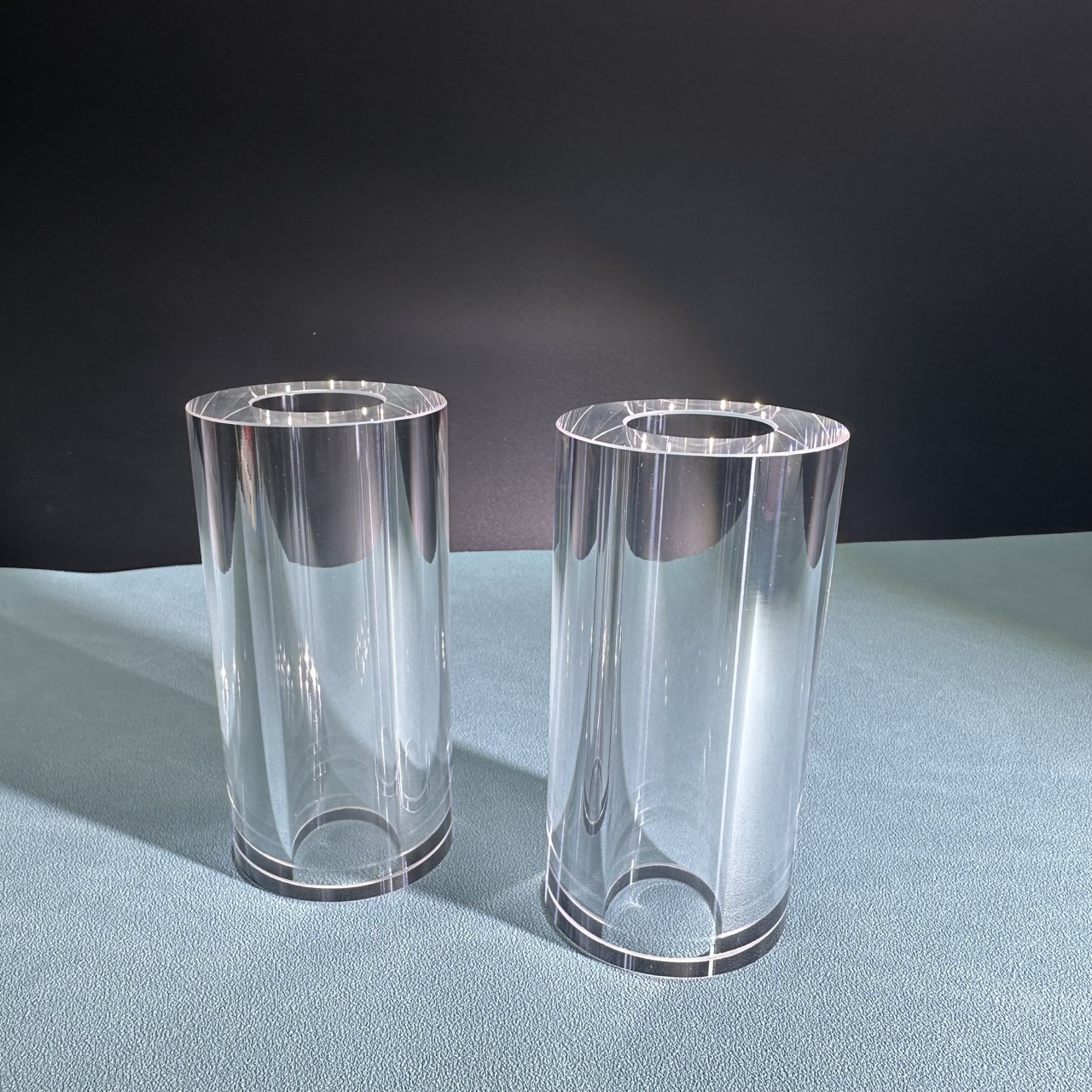
Polished sapphire tubes are precision-engineered components fabricated from single-crystal aluminum oxide (Al₂O₃), a material widely recognized for its exceptional hardness, outstanding optical transparency, and remarkable durability under extreme thermal and chemical environments. Unlike conventional glass or quartz, sapphire tubes deliver superior mechanical strength and long-term stability, making them the preferred choice for critical applications in optics, semiconductors, aerospace, medical devices, and high-temperature systems. Their ability to transmit light effectively across a wide spectrum, from the deep ultraviolet (UV) through the infrared (IR), further enhances their value in scientific and industrial uses.
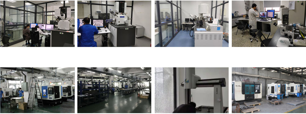
Production & Fabrication Methods
Sapphire tubes are manufactured using two primary crystal growth techniques, each offering unique advantages:
-
EFG (Edge-defined Film-fed Growth):
Produces sapphire tubes directly during the growth stage, forming seamless tubular geometries without excessive machining. This method allows for efficient large-scale production with minimal waste and consistent dimensional accuracy. It is favored for industrial applications where cost efficiency and long lengths are important. -
Kyropoulos (Ky) Method:
Tubes are cut and drilled from carefully grown sapphire boules. Although this process requires more machining, it yields higher crystal uniformity, reduced internal stress, and enhanced optical precision. Ky-method tubes are therefore used in demanding environments such as laser optics, aerospace observation systems, and semiconductor equipment.
Both growth methods are complemented by high-precision polishing, delivering optical-grade surfaces with extremely low roughness (<10 nm Ra), enabling excellent light transmission and mechanical integrity.
Technical Parameters
-
Protective sleeves for optical sensors and laser systems
-
Furnace and reactor tubes for extreme-temperature operations
-
Semiconductor process chambers and components
-
Biomedical and laboratory instrumentation
-
Transparent housings and windows in aerospace and defense systems
-
Spectroscopy setups (UV and IR analysis equipment)
Typical Applications
| Material Property | Value/Description |
|---|---|
| Chemical Formula | Al₂O₃ (aluminum oxide) |
| Hardness | 9 Moh's |
| Class | Hexagonal-scalenohedral |
| Melting Point | 2053°C (3727°F) |
| Maximum Useful Temperature | 2000°C |
| Surface Quality | 80/50, 60/40, 40/20, 20/10 (Scratch/Dig) |
| Axis Orientation | C-Axis (C-Plane), M-Plane, A-Plane, R-Plane and Random |
| Young's Modulus | 435 GPa |
| Tensile Strength | 275 MPa to 400 MPa |
| Flexural Strength | 480 MPa to 895 MPa |
| Modulus of Rigidity | 175 GPa |
| Density | 3.97 g/cm³ |
| Transmission Range | 190nm to 5 microns |
| Poisson's Ratio | 0.27 - 0.30 |
| Abbe Number (νd) | 72.24 |
| Dimension Tolerance | ± 0.01-0.10mm |
| Thickness Tolerance | ± 0.1mm |
FAQ
Q1: What’s the difference between EFG and Ky sapphire tubes?
EFG tubes are grown directly into tubular shapes, offering cost efficiency and long lengths. Ky tubes are machined from boules, offering better crystal consistency and are preferred for precision-demanding applications.
Q2: Can I choose the growth method based on my application?
Yes. If your priority is long, uniform tubes for structural or industrial use, EFG is often more suitable. If high optical quality and lower stress are critical, Ky method may be preferred.
Q3: Are the tubes customizable?
Absolutely. We support custom orders in size, wall thickness, length, crystal orientation, and surface polish.
Q4: What polishing quality do you offer?
We provide optical-grade polishing, with surface roughness typically below 10 nanometers (Ra < 10 nm), ensuring minimal scattering and high transmission.
About Us
XKH specializes in high-tech development, production, and sales of special optical glass and new crystal materials. Our products serve optical electronics, consumer electronics, and the military. We offer Sapphire optical components, mobile phone lens covers, Ceramics, LT, Silicon Carbide SIC, Quartz, and semiconductor crystal wafers. With skilled expertise and cutting-edge equipment, we excel in non-standard product processing, aiming to be a leading optoelectronic materials high-tech enterprise.
Related Products
-

High-Purity Fused Quartz Wafers for Semiconduct...
-
KY and EFG Sapphire Method Tube sapphire rods p...
-
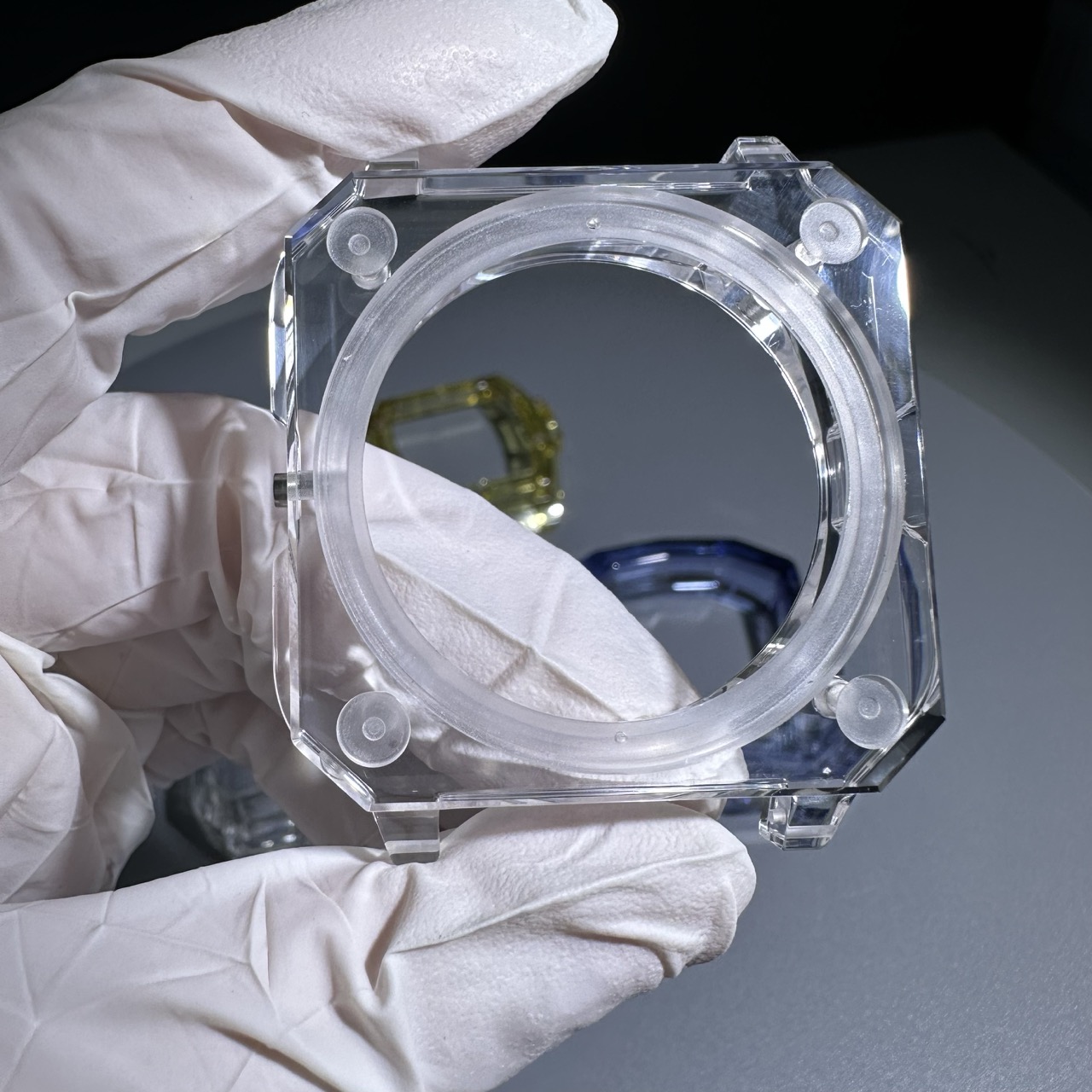
Transparent Sapphire watch case professional cu...
-

BF33 Glass Wafer Advanced Borosilicate Substrat...
-
EFG transparent sapphire tube large outer diame...
-

Custom Sapphire Optical Window 222mm × 74mm × 4...