
Why Semi-Insulating SiC Substrates Are Sensitive to Electromagnetic Interference
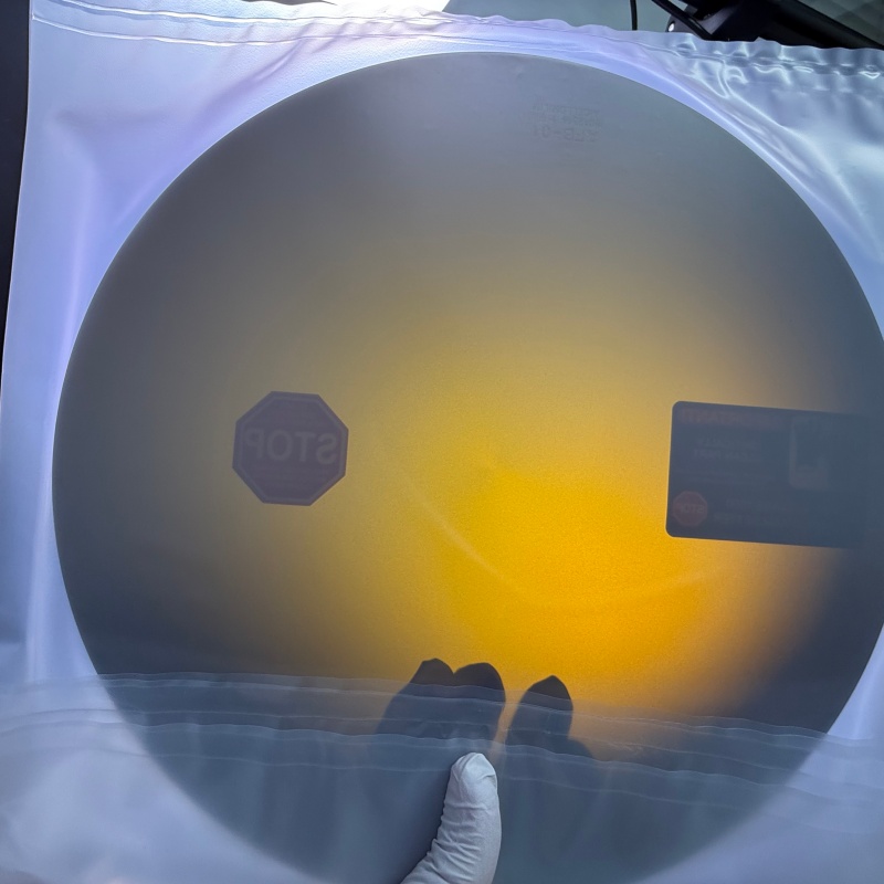
Semi-insulating silicon carbide (SiC) substrates are widely used in high-frequency semiconductor applications, including 5G RF power amplifiers, high-frequency devices, and base station components. With typical resistivity above 1×10⁷ Ω·cm, semi-insulating SiC behaves very differently from conductive SiC when exposed to electromagnetic interference (EMI) and electrostatic effects.
This difference is becoming increasingly important as semiconductor manufacturers demand tighter control over wafer processing environments.
How Does Semi-Insulating SiC Respond to Electromagnetic Fields?
The high resistivity of semi-insulating SiC is commonly achieved through vanadium compensation doping or intrinsic defect compensation mechanisms.
The concentration and distribution of deep-level impurities and crystal defects directly affect resistivity uniformity across the substrate. During processing and inspection, external electromagnetic fields can induce charge redistribution within the wafer.
Potential EMI sources in a semiconductor cleanroom include:
- Variable-frequency drives
- Motors and motion-control systems
- Fan filter units
- Ionizers
- Lighting systems
- Wireless communication equipment
These sources can generate electromagnetic fields ranging from 50 Hz power-frequency fields to GHz-level RF signals.
When semi-insulating SiC is exposed to alternating electromagnetic fields, induced charges and localized current effects can modify the surface electrical potential of the substrate.
Why Does Surface Potential Matter?
Changes in wafer surface potential can influence several downstream processes.
Photolithography
Semi-insulating SiC substrates can act as carriers during photoresist coating. Non-uniform surface potential may affect photoresist spreading and contribute to coating thickness variation.
Chemical Mechanical Planarization
During CMP, surface potential variations may influence abrasive particle adsorption and slurry interaction with the wafer surface, potentially affecting polishing uniformity.
Inspection
Electron-beam and ion-beam inspection systems are particularly sensitive to electromagnetic disturbances. Surface potential fluctuations can reduce imaging accuracy and measurement stability.
Why Cleanroom EMI Control Matters
Conventional cleanrooms are primarily designed to control particles, temperature, humidity, and other environmental parameters. However, these controls alone may not be sufficient for processes involving highly resistive SiC substrates.
For semi-insulating SiC manufacturing, electromagnetic control should be considered alongside contamination control and electrostatic discharge protection.
The goal is not necessarily to shield the entire facility. Instead, shielding requirements should be determined according to wafer exposure conditions, process sensitivity, and equipment electromagnetic susceptibility.
Which Areas Need the Most Protection?
The highest-priority areas generally include:
- Photolithography areas
- CMP areas
- Inspection areas
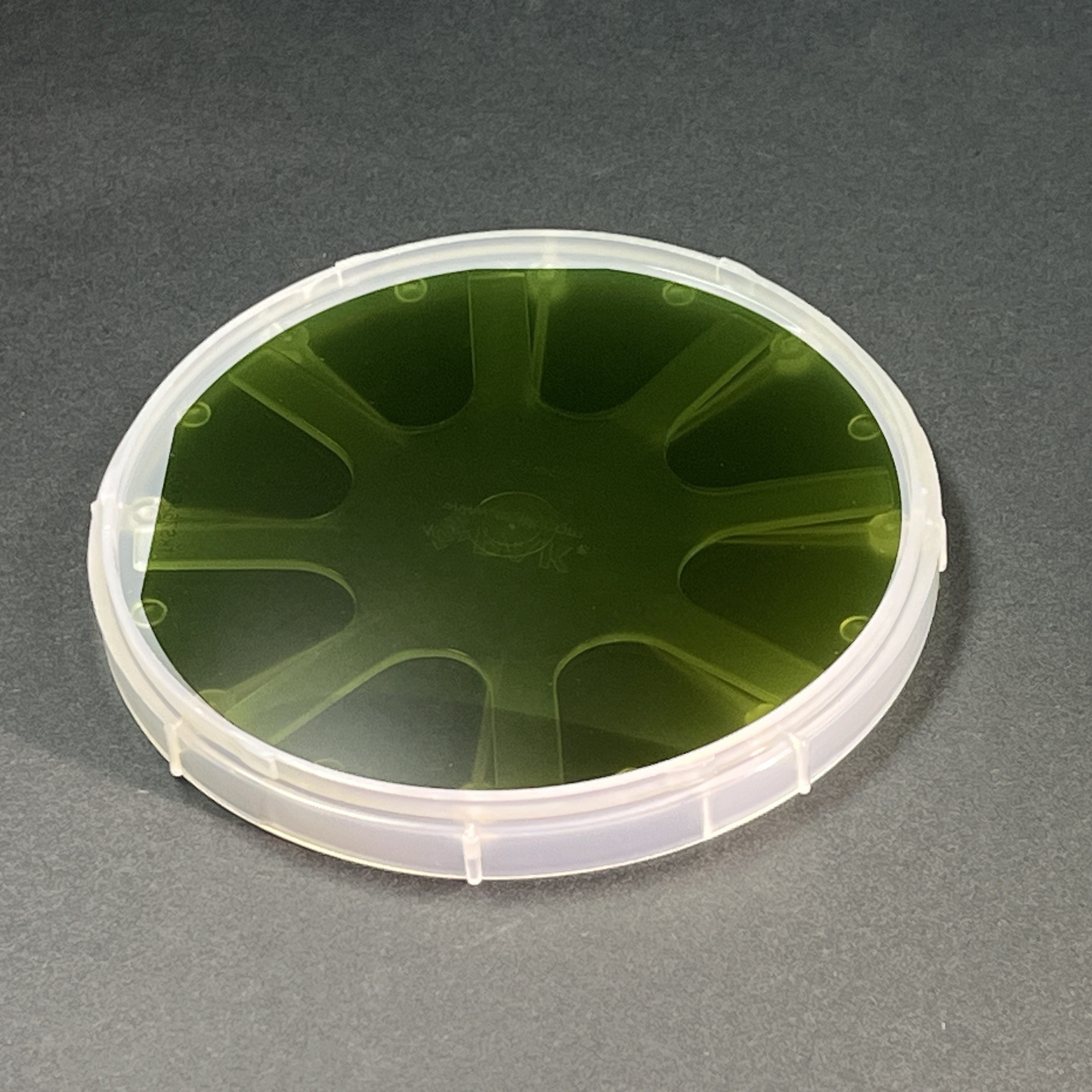
By comparison, storage areas and transfer corridors may require less building-level shielding when wafers remain inside appropriately designed electromagnetic-shielded carriers.
Conclusion
Semi-insulating SiC provides important electrical properties for high-frequency semiconductor applications, but its high resistivity also creates additional environmental-control challenges.
Electromagnetic interference can influence wafer surface potential and potentially affect photoresist coating, CMP stability, and inspection accuracy.
For this reason, EMI management should be considered an integral part of semi-insulating SiC substrate manufacturing, especially in critical process areas.
Post time: Aug-18-2026