SiC wafer's abstract
Silicon carbide (SiC) wafers have become the substrate of choice for high-power, high-frequency, and high-temperature electronics across automotive, renewable energy, and aerospace sectors. Our portfolio covers key polytypes and doping schemes—nitrogen-doped 4H (4H-N), high-purity semi-insulating (HPSI), nitrogen-doped 3C (3C-N), and p-type 4H/6H (4H/6H-P)—offered in three quality grades: PRIME (fully polished, device-grade substrates), DUMMY (lapped or unpolished for process trials), and RESEARCH (custom epi layers and doping profiles for R&D). Wafer diameters span 2″, 4″, 6″, 8″, and 12″ to suit both legacy tools and advanced fabs. We also supply monocrystalline boules and precisely oriented seed crystals to support in-house crystal growth.
Our 4H-N wafers feature carrier densities from 1×10¹⁶ to 1×10¹⁹ cm⁻³ and resistivities of 0.01–10 Ω·cm, delivering excellent electron mobility and breakdown fields above 2 MV/cm—ideal for Schottky diodes, MOSFETs, and JFETs. HPSI substrates exceed 1×10¹² Ω·cm resistivity with micropipe densities below 0.1 cm⁻², ensuring minimal leakage for RF and microwave devices. Cubic 3C-N, available in 2″ and 4″ formats, enables heteroepitaxy on silicon and supports novel photonic and MEMS applications. P-type 4H/6H-P wafers, doped with aluminum to 1×10¹⁶–5×10¹⁸ cm⁻³, facilitate complementary device architectures.
SiC wafer ,PRIME wafers undergo chemical–mechanical polishing to <0.2 nm RMS surface roughness, total thickness variation under 3 µm, and bow <10 µm. DUMMY substrates accelerate assembly and packaging tests, while RESEARCH wafers feature epi-layer thicknesses of 2–30 µm and bespoke doping. All products are certified by X-ray diffraction (rocking curve <30 arcsec) and Raman spectroscopy, with electrical tests—Hall measurements, C–V profiling, and micropipe scanning—ensuring JEDEC and SEMI compliance.
Boules up to 150 mm diameter are grown via PVT and CVD with dislocation densities below 1×10³ cm⁻² and low micropipe counts. Seed crystals are cut within 0.1° of the c-axis to guarantee reproducible growth and high slicing yields.
By combining multiple polytypes, doping variants, quality grades, SiC wafer sizes, and in-house boule and seed-crystal production, our SiC substrate platform streamlines supply chains and accelerates device development for electric vehicles, smart grids, and harsh-environment applications.
SiC wafer‘s abstract
Silicon carbide (SiC) wafers have become the SiC substrate of choice for high-power, high-frequency, and high-temperature electronics across automotive, renewable energy, and aerospace sectors. Our portfolio covers key polytypes and doping schemes—nitrogen-doped 4H (4H-N), high-purity semi-insulating (HPSI), nitrogen-doped 3C (3C-N), and p-type 4H/6H (4H/6H-P)—offered in three quality grades:SiC wafer PRIME (fully polished, device-grade substrates), DUMMY (lapped or unpolished for process trials), and RESEARCH (custom epi layers and doping profiles for R&D). SiC Wafer diameters span 2″, 4″, 6″, 8″, and 12″ to suit both legacy tools and advanced fabs. We also supply monocrystalline boules and precisely oriented seed crystals to support in-house crystal growth.
Our 4H-N SiC wafers feature carrier densities from 1×10¹⁶ to 1×10¹⁹ cm⁻³ and resistivities of 0.01–10 Ω·cm, delivering excellent electron mobility and breakdown fields above 2 MV/cm—ideal for Schottky diodes, MOSFETs, and JFETs. HPSI substrates exceed 1×10¹² Ω·cm resistivity with micropipe densities below 0.1 cm⁻², ensuring minimal leakage for RF and microwave devices. Cubic 3C-N, available in 2″ and 4″ formats, enables heteroepitaxy on silicon and supports novel photonic and MEMS applications. SiC wafer P-type 4H/6H-P wafers, doped with aluminum to 1×10¹⁶–5×10¹⁸ cm⁻³, facilitate complementary device architectures.
SiC wafer PRIME wafers undergo chemical–mechanical polishing to <0.2 nm RMS surface roughness, total thickness variation under 3 µm, and bow <10 µm. DUMMY substrates accelerate assembly and packaging tests, while RESEARCH wafers feature epi-layer thicknesses of 2–30 µm and bespoke doping. All products are certified by X-ray diffraction (rocking curve <30 arcsec) and Raman spectroscopy, with electrical tests—Hall measurements, C–V profiling, and micropipe scanning—ensuring JEDEC and SEMI compliance.
Boules up to 150 mm diameter are grown via PVT and CVD with dislocation densities below 1×10³ cm⁻² and low micropipe counts. Seed crystals are cut within 0.1° of the c-axis to guarantee reproducible growth and high slicing yields.
By combining multiple polytypes, doping variants, quality grades, SiC wafer sizes, and in-house boule and seed-crystal production, our SiC substrate platform streamlines supply chains and accelerates device development for electric vehicles, smart grids, and harsh-environment applications.
SiC wafer‘s picture


6inch 4H-N type SiC wafer‘s data sheet
| 6inch SiC wafers data sheet | ||||
| Parameter | Sub-Parameter | Z Grade | P Grade | D Grade |
| Diameter | 149.5–150.0 mm | 149.5–150.0 mm | 149.5–150.0 mm | |
| Thickness | 4H‑N | 350 µm ± 15 µm | 350 µm ± 25 µm | 350 µm ± 25 µm |
| Thickness | 4H‑SI | 500 µm ± 15 µm | 500 µm ± 25 µm | 500 µm ± 25 µm |
| Wafer Orientation | Off axis: 4.0° toward <11-20> ±0.5° (4H-N); On axis: <0001> ±0.5° (4H-SI) | Off axis: 4.0° toward <11-20> ±0.5° (4H-N); On axis: <0001> ±0.5° (4H-SI) | Off axis: 4.0° toward <11-20> ±0.5° (4H-N); On axis: <0001> ±0.5° (4H-SI) | |
| Micropipe Density | 4H‑N | ≤ 0.2 cm⁻² | ≤ 2 cm⁻² | ≤ 15 cm⁻² |
| Micropipe Density | 4H‑SI | ≤ 1 cm⁻² | ≤ 5 cm⁻² | ≤ 15 cm⁻² |
| Resistivity | 4H‑N | 0.015–0.024 Ω·cm | 0.015–0.028 Ω·cm | 0.015–0.028 Ω·cm |
| Resistivity | 4H‑SI | ≥ 1×10¹⁰ Ω·cm | ≥ 1×10⁵ Ω·cm | |
| Primary Flat Orientation | [10-10] ± 5.0° | [10-10] ± 5.0° | [10-10] ± 5.0° | |
| Primary Flat Length | 4H‑N | 47.5 mm ± 2.0 mm | ||
| Primary Flat Length | 4H‑SI | Notch | ||
| Edge Exclusion | 3 mm | |||
| Warp/LTV/TTV/Bow | ≤2.5 µm / ≤6 µm / ≤25 µm / ≤35 µm | ≤5 µm / ≤15 µm / ≤40 µm / ≤60 µm | ||
| Roughness | Polish | Ra ≤ 1 nm | ||
| Roughness | CMP | Ra ≤ 0.2 nm | Ra ≤ 0.5 nm | |
| Edge Cracks | None | Cumulative length ≤ 20 mm, single ≤ 2 mm | ||
| Hex Plates | Cumulative area ≤ 0.05% | Cumulative area ≤ 0.1% | Cumulative area ≤ 1% | |
| Polytype Areas | None | Cumulative area ≤ 3% | Cumulative area ≤ 3% | |
| Carbon Inclusions | Cumulative area ≤ 0.05% | Cumulative area ≤ 3% | ||
| Surface Scratches | None | Cumulative length ≤ 1 × wafer diameter | ||
| Edge Chips | None permitted ≥ 0.2 mm width & depth | Up to 7 chips, ≤ 1 mm each | ||
| TSD (Threading Screw Dislocation) | ≤ 500 cm⁻² | N/A | ||
| BPD (Base Plane Dislocation) | ≤ 1000 cm⁻² | N/A | ||
| Surface Contamination | None | |||
| Packaging | Multi-wafer cassette or single wafer container | Multi-wafer cassette or single wafer container | Multi-wafer cassette or single wafer container | |
4inch 4H-N type SiC wafer‘s data sheet
| 4inch SiC wafer's data sheet | |||
| Parameter | Zero MPD Production | Standard Production Grade (P Grade) | Dummy Grade (D Grade) |
| Diameter | 99.5 mm–100.0 mm | ||
| Thickness (4H-N) | 350 µm±15 µm | 350 µm±25 µm | |
| Thickness (4H-Si) | 500 µm±15 µm | 500 µm±25 µm | |
| Wafer Orientation | Off axis: 4.0° toward <1120> ±0.5° for 4H-N; On axis: <0001> ±0.5° for 4H-Si | ||
| Micropipe Density (4H-N) | ≤0.2 cm⁻² | ≤2 cm⁻² | ≤15 cm⁻² |
| Micropipe Density (4H-Si) | ≤1 cm⁻² | ≤5 cm⁻² | ≤15 cm⁻² |
| Resistivity (4H-N) | 0.015–0.024 Ω·cm | 0.015–0.028 Ω·cm | |
| Resistivity (4H-Si) | ≥1E10 Ω·cm | ≥1E5 Ω·cm | |
| Primary Flat Orientation | [10-10] ±5.0° | ||
| Primary Flat Length | 32.5 mm ±2.0 mm | ||
| Secondary Flat Length | 18.0 mm ±2.0 mm | ||
| Secondary Flat Orientation | Silicon face up: 90° CW from prime flat ±5.0° | ||
| Edge Exclusion | 3 mm | ||
| LTV/TTV/Bow Warp | ≤2.5 µm/≤5 µm/≤15 µm/≤30 µm | ≤10 µm/≤15 µm/≤25 µm/≤40 µm | |
| Roughness | Polish Ra ≤1 nm; CMP Ra ≤0.2 nm | Ra ≤0.5 nm | |
| Edge Cracks By High Intensity Light | None | None | Cumulative length ≤10 mm; single length ≤2 mm |
| Hex Plates By High Intensity Light | Cumulative area ≤0.05% | Cumulative area ≤0.05% | Cumulative area ≤0.1% |
| Polytype Areas By High Intensity Light | None | Cumulative area ≤3% | |
| Visual Carbon Inclusions | Cumulative area ≤0.05% | Cumulative area ≤3% | |
| Silicon Surface Scratches By High Intensity Light | None | Cumulative length ≤1 wafer diameter | |
| Edge Chips By High Intensity Light | None permitted ≥0.2 mm width and depth | 5 allowed, ≤1 mm each | |
| Silicon Surface Contamination By High Intensity Light | None | ||
| Threading screw dislocation | ≤500 cm⁻² | N/A | |
| Packaging | Multi-wafer cassette or single wafer container | Multi-wafer cassette or single wafer container | Multi-wafer cassette or single wafer container |
4inch HPSI type SiC wafer‘s data sheet
| 4inch HPSI type SiC wafer's data sheet | |||
| Parameter | Zero MPD Production Grade (Z Grade) | Standard Production Grade (P Grade) | Dummy Grade (D Grade) |
| Diameter | 99.5–100.0 mm | ||
| Thickness (4H-Si) | 500 µm ±20 µm | 500 µm ±25 µm | |
| Wafer Orientation | Off axis: 4.0° toward <11-20> ±0.5° for 4H-N; On axis: <0001> ±0.5° for 4H-Si | ||
| Micropipe Density (4H-Si) | ≤1 cm⁻² | ≤5 cm⁻² | ≤15 cm⁻² |
| Resistivity (4H-Si) | ≥1E9 Ω·cm | ≥1E5 Ω·cm | |
| Primary Flat Orientation | (10-10) ±5.0° | ||
| Primary Flat Length | 32.5 mm ±2.0 mm | ||
| Secondary Flat Length | 18.0 mm ±2.0 mm | ||
| Secondary Flat Orientation | Silicon face up: 90° CW from prime flat ±5.0° | ||
| Edge Exclusion | 3 mm | ||
| LTV/TTV/Bow Warp | ≤3 µm/≤5 µm/≤15 µm/≤30 µm | ≤10 µm/≤15 µm/≤25 µm/≤40 µm | |
| Roughness (C face) | Polish | Ra ≤1 nm | |
| Roughness (Si face) | CMP | Ra ≤0.2 nm | Ra ≤0.5 nm |
| Edge Cracks By High Intensity Light | None | Cumulative length ≤10 mm; single length ≤2 mm | |
| Hex Plates By High Intensity Light | Cumulative area ≤0.05% | Cumulative area ≤0.05% | Cumulative area ≤0.1% |
| Polytype Areas By High Intensity Light | None | Cumulative area ≤3% | |
| Visual Carbon Inclusions | Cumulative area ≤0.05% | Cumulative area ≤3% | |
| Silicon Surface Scratches By High Intensity Light | None | Cumulative length ≤1 wafer diameter | |
| Edge Chips By High Intensity Light | None permitted ≥0.2 mm width and depth | 5 allowed, ≤1 mm each | |
| Silicon Surface Contamination By High Intensity Light | None | None | |
| Threading Screw Dislocation | ≤500 cm⁻² | N/A | |
| Packaging | Multi-wafer cassette or single wafer container | ||
SiC wafer's application
-
SiC Wafer Power Modules for EV Inverters
SiC wafer-based MOSFETs and diodes built on high-quality SiC wafer substrates deliver ultra-low switching losses. By leveraging SiC wafer technology, these power modules operate at higher voltages and temperatures, enabling more efficient traction inverters. Integrating SiC wafer dies into power stages reduces cooling requirements and footprint, showcasing the full potential of SiC wafer innovation. -
High-Frequency RF & 5G Devices on SiC Wafer
RF amplifiers and switches fabricated on semi-insulating SiC wafer platforms exhibit superior thermal conductivity and breakdown voltage. The SiC wafer substrate minimizes dielectric losses at GHz frequencies, while SiC wafer’s material strength allows for stable operation under high-power, high-temperature conditions—making SiC wafer the substrate of choice for next-gen 5G base stations and radar systems. -
Optoelectronic & LED Substrates from SiC Wafer
Blue and UV LEDs grown on SiC wafer substrates benefit from excellent lattice matching and heat dissipation. Using a polished C-face SiC wafer ensures uniform epitaxial layers, while the inherent hardness of SiC wafer enables fine wafer thinning and reliable device packaging. This makes SiC wafer the go-to platform for high-power, long-lifetime LED applications.
SiC wafer's Q&A
1. Q: How are SiC wafers manufactured?
A:
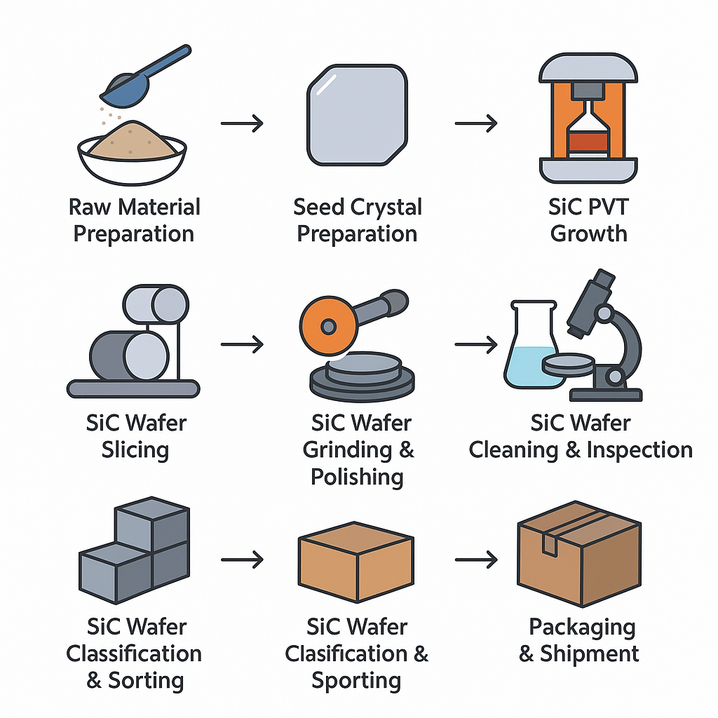
SiC wafers manufactured Detailed Steps
-
SiC wafers Raw Material Preparation
- Use ≥5N-grade SiC powder (impurities ≤1 ppm).
- Sieve and pre-bake to remove residual carbon or nitrogen compounds.
-
SiC Seed Crystal Preparation
-
Take a piece of 4H-SiC single crystal, slice along the 〈0001〉 orientation to ~10 × 10 mm².
-
Precision polish to Ra ≤0.1 nm and mark crystal orientation.
-
-
SiC PVT Growth (Physical Vapor Transport)
-
Load graphite crucible: bottom with SiC powder, top with seed crystal.
-
Evacuate to 10⁻³–10⁻⁵ Torr or backfill with high-purity helium at 1 atm.
-
Heat source zone to 2100–2300 ℃, maintain seed zone 100–150 ℃ cooler.
-
Control growth rate at 1–5 mm/h to balance quality and throughput.
-
-
SiC Ingot Annealing
-
Anneal the as-grown SiC ingot at 1600–1800 ℃ for 4–8 hours.
-
Purpose: relieve thermal stresses and reduce dislocation density.
-
-
SiC Wafer Slicing
-
Use a diamond wire saw to slice the ingot into 0.5–1 mm thick wafers.
-
Minimize vibration and lateral force to avoid micro-cracks.
-
-
SiC Wafer Grinding & Polishing
-
Coarse grinding to remove sawing damage (roughness ~10–30 µm).
-
Fine grinding to achieve flatness ≤5 µm.
-
Chemical-Mechanical Polishing (CMP) to reach mirror-like finish (Ra ≤0.2 nm).
-
-
SiC Wafer Cleaning & Inspection
-
Ultrasonic cleaning in Piranha solution (H₂SO₄:H₂O₂), DI water, then IPA.
-
XRD/Raman spectroscopy to confirm polytype (4H, 6H, 3C).
-
Interferometry to measure flatness (<5 µm) and warp (<20 µm).
-
Four-point probe to test resistivity (e.g. HPSI ≥10⁹ Ω·cm).
-
Defect inspection under polarized light microscope and scratch tester.
-
-
SiC Wafer Classification & Sorting
-
Sort wafers by polytype and electrical type:
-
4H-SiC N-type (4H-N): carrier concentration 10¹⁶–10¹⁸ cm⁻³
-
4H-SiC High Purity Semi-Insulating (4H-HPSI): resistivity ≥10⁹ Ω·cm
-
6H-SiC N-type (6H-N)
-
Others: 3C-SiC, P-type, etc.
-
-
-
SiC Wafer Packaging & Shipment
-
Place in clean, dust-free wafer boxes.
-
Label each box with diameter, thickness, polytype, resistivity grade, and batch number.
-
2. Q: What are the key advantages of SiC wafers over silicon wafers?
A: Compared to silicon wafers, SiC wafers enable:
-
Higher voltage operation (>1,200 V) with lower on-resistance.
-
Higher temperature stability (>300 °C) and improved thermal management.
-
Faster switching speeds with lower switching losses, reducing system-level cooling and size in power converters.
4. Q: What common defects affect SiC wafer yield and performance?
A: The primary defects in SiC wafers include micropipes, basal plane dislocations (BPDs), and surface scratches. Micropipes can cause catastrophic device failure; BPDs increase on-resistance over time; and surface scratches lead to wafer breakage or poor epitaxial growth. Rigorous inspection and defect mitigation are therefore essential to maximize SiC wafer yield.
Post time: Jun-30-2025