
How to Design Electromagnetic Shielding for a Semi-Insulating SiC Cleanroom
Electromagnetic shielding is becoming an important consideration in cleanroom design for semi-insulating SiC substrate manufacturing.
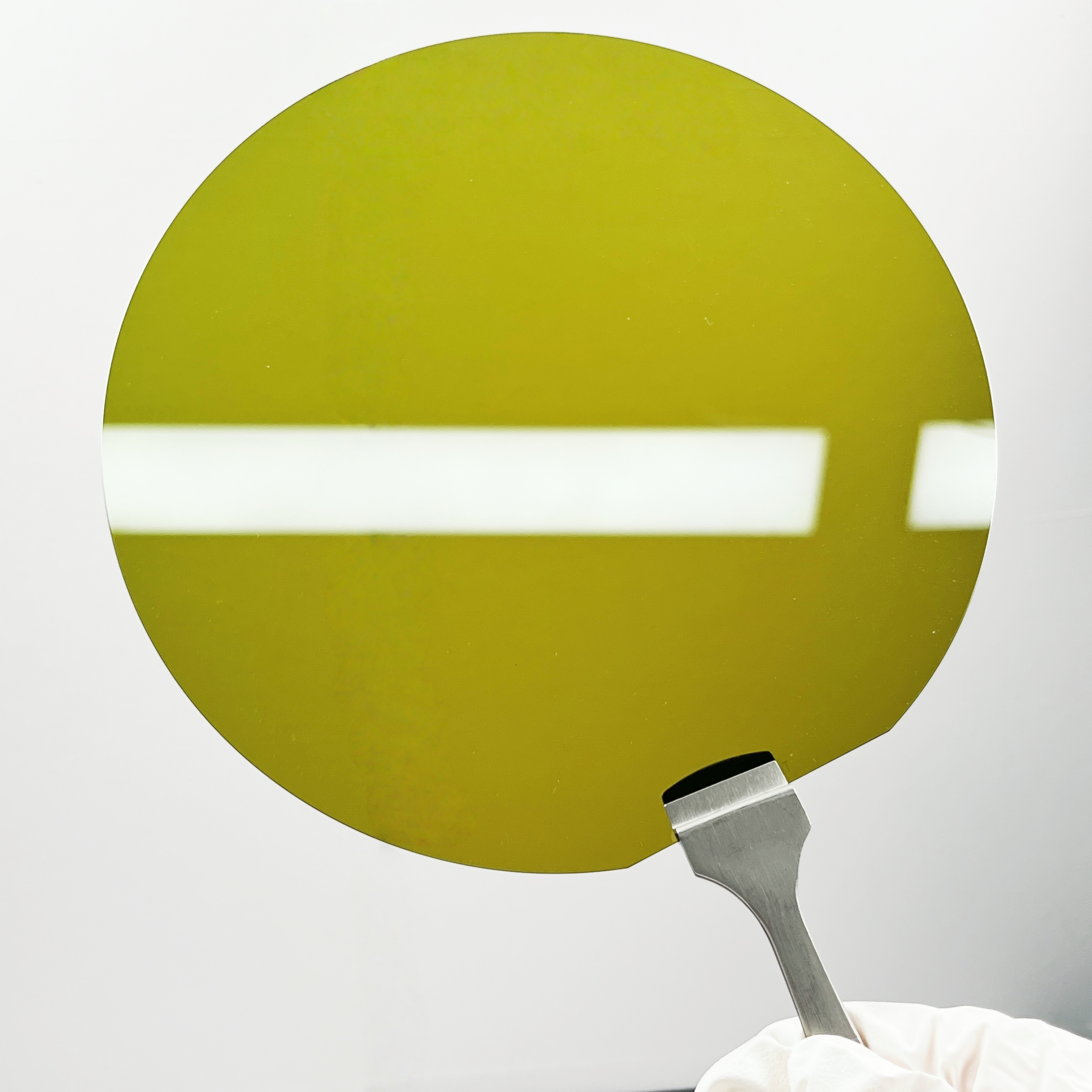
Because semi-insulating SiC substrates have high electrical resistivity, external electromagnetic fields can affect charge distribution and surface electrical potential. Proper shielding design can help reduce these disturbances in sensitive semiconductor processes.
Does the Entire Cleanroom Need Electromagnetic Shielding?
Not necessarily.
A semi-insulating SiC cleanroom should be divided according to substrate exposure conditions, process sensitivity, and equipment electromagnetic susceptibility.
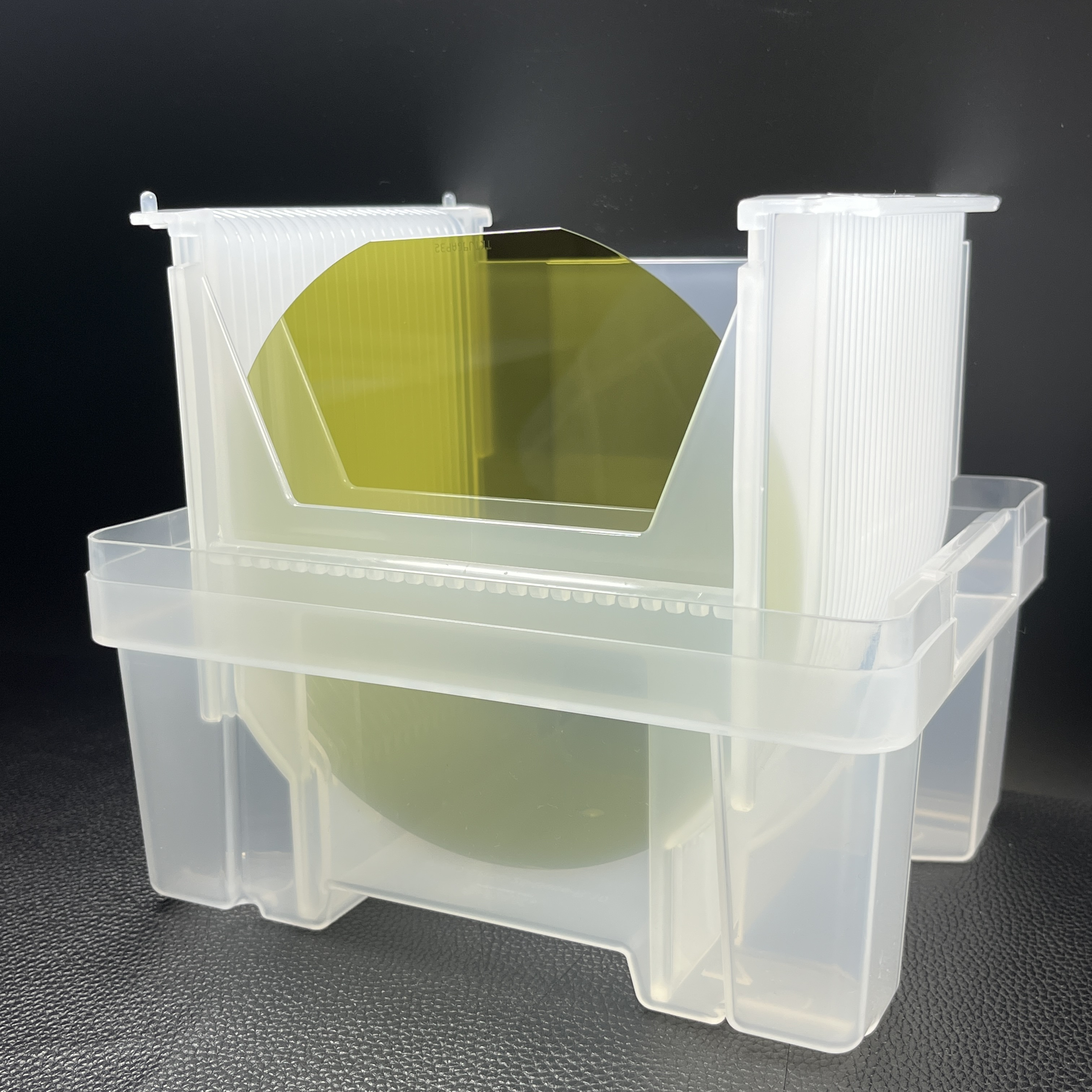
When wafers remain inside sealed carriers, the carrier itself can provide a certain level of electromagnetic protection. Conductive polymer materials or metal-coated polymer structures may be used for wafer carriers, and the carrier housing should be electrically grounded.
Once wafers are removed from the carrier and exposed directly to the cleanroom environment, building-level shielding becomes more important.
Critical Areas for Electromagnetic Shielding
Photolithography Area
After photoresist coating, the substrate surface can become particularly sensitive to electrical potential variations. Electromagnetic shielding can help maintain coating uniformity and lithography accuracy.
CMP Area
Surface potential control is important for maintaining stable slurry behavior and consistent polishing performance.
Inspection Area
Electron-beam and ion-beam inspection systems are highly sensitive to electromagnetic disturbances. Independent shielding protection is therefore recommended for critical inspection areas.
Common Shielding Structures
Cleanroom electromagnetic shielding structures can incorporate:
- Metal plates
- Metal mesh layers
- Embedded conductive shielding structures
These structures can be installed in walls, ceilings, and floors.
Common shielding materials include:
- Copper foil
- Galvanized steel sheets
- Stainless steel plates
The thickness and structure of the shielding layer should be selected according to the required shielding effectiveness and target frequency range.
Target Shielding Effectiveness
Different frequency ranges require different shielding targets.
| Frequency Range | Target Shielding Effectiveness |
|---|---|
| Power-frequency magnetic field | ≥20 dB |
| RF electric field, 1 MHz–1 GHz | ≥40 dB |
| Microwave frequency, >1 GHz | ≥30 dB |
The actual targets should be determined according to whether electromagnetic exposure at specific frequencies could generate sufficient induced charge to affect process stability or yield.
Maintaining Shielding Continuity
A shielding layer is only effective when its electrical continuity is properly maintained.
Important design considerations include:
- Conductive gaskets or conductive adhesive tapes at panel joints
- Overlapping shielding structures by at least 50 mm
- Waveguide ventilation windows for openings
- Conductive sealing strips on doors
- Full-perimeter electrical contact between door frames and sealing strips
Small discontinuities, gaps, or poorly designed openings can reduce overall shielding performance.
Grounding the Shielding System
The shielding layer should use a low-impedance grounding system with single-point grounding.
A recommended ground resistance is ≤1 Ω.
Multiple grounding points may create ground loops. Induced currents flowing through these loops can generate secondary magnetic fields and reduce the effectiveness of the shielding system.
Conclusion
Effective electromagnetic shielding for semi-insulating SiC manufacturing is not simply a matter of adding metal panels to a cleanroom.
A successful design must integrate shielding materials, structural continuity, openings, doors, grounding, wafer carriers, and process zoning.
By focusing shielding resources on photolithography, CMP, and inspection areas, semiconductor manufacturers can build a more targeted electromagnetic-control environment while avoiding unnecessary shielding throughout the entire facility.
Post time: Aug-12-2026