Semiconductor materials have evolved through three transformative generations:
1st Gen (Si/Ge) laid the foundation of modern electronics,
2nd Gen (GaAs/InP) broke through optoelectronic and high-frequency barriers to power the information revolution,
3rd Gen (SiC/GaN) now tackles energy and extreme-environment challenges, enabling carbon neutrality and 6G era.
This progression reveals a paradigm shift from versatility to specialization in material science.
1. First-Generation Semiconductors: Silicon (Si) and Germanium (Ge)
Historical Background
In 1947, Bell Labs invented the germanium transistor, marking the dawn of the semiconductor era. By the 1950s, silicon gradually replaced germanium as the foundation of integrated circuits (ICs) due to its stable oxide layer (SiO₂) and abundant natural reserves.
Material Properties
Ⅰ Bandgap:
Germanium: 0.67eV (narrow bandgap, prone to leakage current, poor high-temperature performance).
Silicon: 1.12eV (indirect bandgap, suitable for logic circuits but incapable of light emission).
Ⅱ、Advantages of Silicon:
Naturally forms a high-quality oxide (SiO₂), enabling MOSFET fabrication.
Low cost and earth-abundant (~28% of crustal composition).
Ⅲ、Limitations:
Low electron mobility (only 1500 cm²/(V·s)), restricting high-frequency performance.
Weak voltage/temperature tolerance (max operating temp. ~150°C).
Key Applications
Ⅰ、Integrated Circuits (ICs):
CPUs, memory chips (e.g., DRAM, NAND) rely on silicon for high integration density.
Example: Intel’s 4004 (1971), the first commercial microprocessor, used 10μm silicon technology.
Ⅱ、Power Devices:
Early thyristors and low-voltage MOSFETs (e.g., PC power supplies) were silicon-based.
Challenges & Obsolescence
Germanium was phased out due to leakage and thermal instability. However, silicon’s limitations in optoelectronics and high-power applications spurred the development of next-gen semiconductors.
2Second-Generation Semiconductors: Gallium Arsenide (GaAs) and Indium Phosphide (InP)
Development Background
During the 1970s–1980s, emerging fields like mobile communications, optical fiber networks, and satellite technology created a pressing demand for high-frequency and efficient optoelectronic materials. This drove the advancement of direct bandgap semiconductors like GaAs and InP.
Material Properties
Bandgap & Optoelectronic Performance:
GaAs: 1.42eV (direct bandgap, enables light emission—ideal for lasers/LEDs).
InP: 1.34eV (better suited for long-wavelength applications, e.g., 1550nm fiber-optic communications).
Electron Mobility:
GaAs achieves 8500 cm²/(V·s), far surpassing silicon (1500 cm²/(V·s)), making it optimal for GHz-range signal processing.
Disadvantages
l Brittle substrates: Harder to manufacture than silicon; GaAs wafers cost 10× more.
l No native oxide: Unlike silicon’s SiO₂, GaAs/InP lack stable oxides, hindering high-density IC fabrication.
Key Applications
l RF Front-Ends:
Mobile power amplifiers (PAs), satellite transceivers (e.g., GaAs-based HEMT transistors).
l Optoelectronics:
Laser diodes (CD/DVD drives), LEDs (red/infrared), fiber-optic modules (InP lasers).
l Space Solar Cells:
GaAs cells achieve 30% efficiency (vs. ~20% for silicon), crucial for satellites.
l Technological Bottlenecks
High costs confine GaAs/InP to niche high-end applications, preventing them from displacing silicon’s dominance in logic chips.
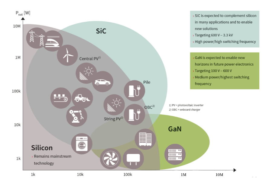
Third-Generation Semiconductors (Wide-Bandgap Semiconductors): Silicon Carbide (SiC) and Gallium Nitride (GaN)
Technology Drivers
Energy Revolution: Electric vehicles and renewable energy grid integration demand more efficient power devices.
High-Frequency Needs: 5G communications and radar systems require higher frequencies and power density.
Extreme Environments: Aerospace and industrial motor applications need materials capable of withstanding temperatures exceeding 200°C.
Material Characteristics
Wide Bandgap Advantages:
l SiC: Bandgap of 3.26eV, breakdown electric field strength 10× that of silicon, capable of withstanding voltages over 10kV.
l GaN: Bandgap of 3.4eV, electron mobility of 2200 cm²/(V·s), excelling in high-frequency performance.
Thermal Management:
SiC’s thermal conductivity reaches 4.9 W/(cm·K), three times better than silicon, making it ideal for high-power applications.
Material Challenges
SiC: Slow single-crystal growth requires temperatures above 2000°C, resulting in wafer defects and high costs (a 6-inch SiC wafer is 20× more expensive than silicon).
GaN: Lacks a natural substrate, often requiring heteroepitaxy on sapphire, SiC, or silicon substrates, leading to lattice mismatch issues.
Key Applications
Power Electronics:
EV inverters (e.g., Tesla Model 3 uses SiC MOSFETs, improving efficiency by 5–10%).
Fast-charging stations/adapters (GaN devices enable 100W+ fast charging while reducing size by 50%).
RF Devices:
5G base station power amplifiers (GaN-on-SiC PAs support mmWave frequencies).
Military radar (GaN offers 5× the power density of GaAs).
Optoelectronics:
UV LEDs (AlGaN materials used in sterilization and water quality detection).
Industry Status and Future Outlook
SiC dominates the high-power market, with automotive-grade modules already in mass production, though costs remain a barrier.
GaN is rapidly expanding in consumer electronics (fast charging) and RF applications, transitioning toward 8-inch wafers.
Emerging materials like gallium oxide (Ga₂O₃, bandgap 4.8eV) and diamond (5.5eV) may form a “fourth generation” of semiconductors, pushing voltage limits beyond 20kV.
Coexistence and Synergy of Semiconductor Generations
Complementarity, Not Replacement:
Silicon remains dominant in logic chips and consumer electronics (95% of the global semiconductor market).
GaAs and InP specialize in high-frequency and optoelectronic niches.
SiC/GaN are irreplaceable in energy and industrial applications.
Technology Integration Examples:
GaN-on-Si: Combines GaN with low-cost silicon substrates for fast charging and RF applications.
SiC-IGBT hybrid modules: Improve grid conversion efficiency.
Future Trends:
Heterogeneous integration: Combining materials (e.g., Si + GaN) on a single chip to balance performance and cost.
Ultra-wide bandgap materials (e.g., Ga₂O₃, diamond) may enable ultra-high-voltage (>20kV) and quantum computing applications.
Related production
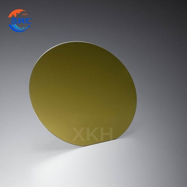
GaAs laser epitaxial wafer 4 inch 6 inch
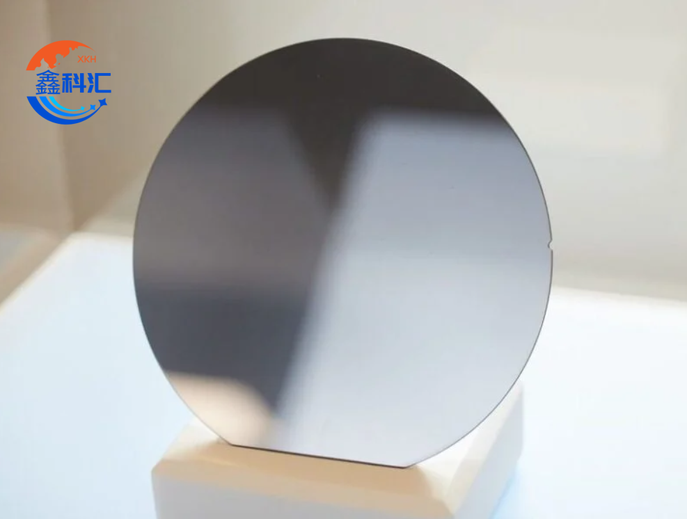
12 inch SIC substrate silicon carbide prime grade diameter 300mm large size 4H-N Suitable for high power device heat dissipation
Post time: May-07-2025