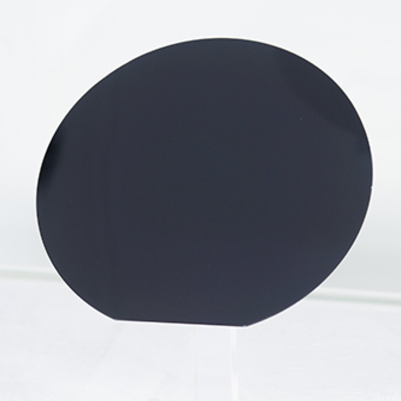
LiTaO3 Wafer 2inch-8inch 10x10x0.5 mm 1sp 2sp for 5G/6G Communications
Technical parameters
| Name | Optical-grade LiTaO3 | Sound table level LiTaO3 |
| Axial | Z cut + / - 0.2 ° | 36 ° Y cut / 42 ° Y cut / X cut
(+ / - 0.2 °) |
| Diameter | 76.2mm + / - 0.3mm/
100±0.2mm |
76.2mm + /-0.3mm
100mm + /-0.3mm 0r 150±0.5mm |
| Datum plane | 22mm + / - 2mm | 22mm + /-2mm
32mm + /-2mm |
| Thickness | 500um + /-5mm
1000um + /-5mm |
500um + /-20mm
350um + /-20mm |
| TTV | ≤ 10um | ≤ 10um |
| Curie temperature | 605 °C + / - 0.7 °C (DTAmethod) | 605 °C + / -3 °C (DTAmethod |
| Surface quality | Double-sided polishing | Double-sided polishing |
| Chamfered edges | edge rounding | edge rounding |
Key Characteristics
1.Electrical and Optical Performance
· Electro-Optic Coefficient: r33 reaches 30 pm/V (X-cut), 1.5× higher than LiNbO3, enabling ultra-wideband electro-optic modulation (>40 GHz bandwidth).
· Broad Spectral Response: Transmission range 0.4–5.0 μm (8 mm thickness), with ultraviolet absorption edge as low as 280 nm, ideal for UV lasers and quantum dot devices.
· Low Pyroelectric Coefficient: dP/dT = 3.5×10⁻⁴ C/(m²·K), ensuring stability in high-temperature infrared sensors.
2.Thermal and Mechanical Properties
· High Thermal Conductivity: 4.6 W/m·K (X-cut), quadruple that of quartz, sustaining -200–500°C thermal cycling.
· Low Thermal Expansion Coefficient: CTE = 4.1×10⁻⁶/K (25–1000°C), compatible with silicon packaging to minimize thermal stress.
3.Defect Control and Processing Precision
· Micropipe Density: <0.1 cm⁻² (8-inch wafers), dislocation density <500 cm⁻² (verified via KOH etching).
· Surface Quality: CMP-polished to Ra <0.5 nm, meeting EUV lithography-grade flatness requirements.
Key Applications
|
Domain |
Application Scenarios |
Technical Advantages |
|
Optical Communications |
100G/400G DWDM lasers, silicon photonics hybrid modules |
LiTaO3 wafer’s broad spectral transmission and low waveguide loss (α <0.1 dB/cm) enable C-band expansion. |
|
5G/6G Communications |
SAW filters (1.8–3.5 GHz), BAW-SMR filters |
42°Y-cut wafers achieve Kt² >15%, delivering low insertion loss (<1.5 dB) and high roll-off (>30 dB). |
|
Quantum Technologies |
Single-photon detectors, parametric down-conversion sources |
High nonlinear coefficient (χ(2)=40 pm/V) and low dark count rate (<100 counts/s) enhance quantum fidelity. |
|
Industrial Sensing |
High-temperature pressure sensors, current transformers |
LiTaO3 wafer’s piezoelectric response (g33 >20 mV/m) and high-temperature tolerance (>400°C) suit extreme environments. |
XKH Services
1.Custom Wafer Fabrication
· Size and Cutting: 2–8-inch wafers with X/Y/Z-cut, 42°Y-cut, and custom angular cuts (±0.01° tolerance).
· Doping Control: Fe, Mg doping via Czochralski method (concentration range 10¹⁶–10¹⁹ cm⁻³) to optimize electro-optic coefficients and thermal stability.
2.Advanced Process Technologies
· Periodic Poling (PPLT): Smart-Cut technology for LTOI wafers, achieving ±10 nm domain period precision and quasi-phase-matched (QPM) frequency conversion.
· Heterogeneous Integration: Si-based LiTaO3 composite wafers (POI) with thickness control (300–600 nm) and thermal conductivity up to 8.78 W/m·K for high-frequency SAW filters.
3.Quality Management Systems
· End-to-End Testing: Raman spectroscopy (polytype verification), XRD (crystallinity), AFM (surface morphology), and optical uniformity testing (Δn <5×10⁻⁵).
4.Global Supply Chain Support
· Production Capacity: Monthly output >5,000 wafers (8-inch: 70%), with 48-hour emergency delivery.
· Logistics Network: Coverage in Europe, North America, and Asia-Pacific via air/sea freight with temperature-controlled packaging.


