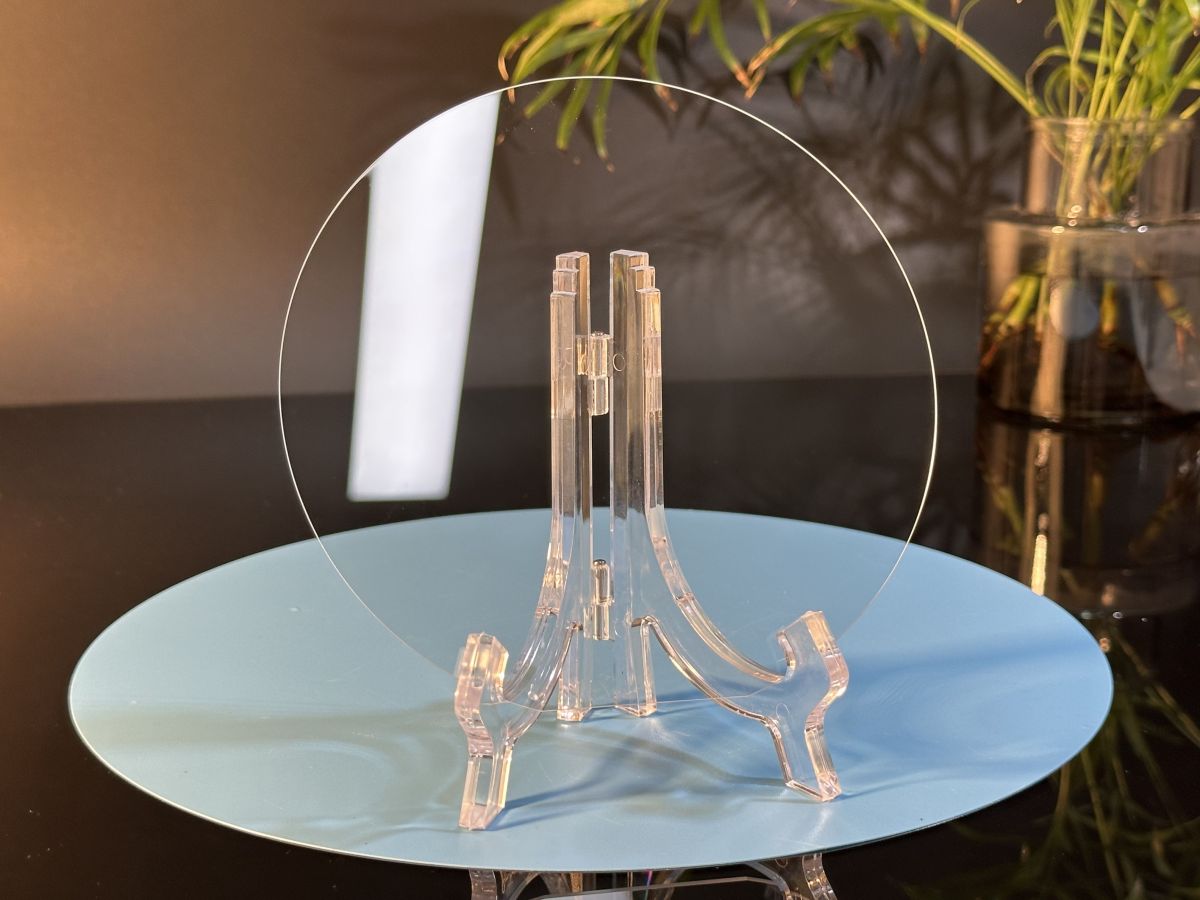
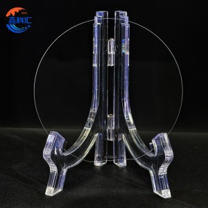
12inch Sapphire Wafer C-Plane SSP/DSP

Detailed Diagram
Sapphire Introduction
Sapphire wafer is a single-crystal substrate material made from high-purity synthetic aluminum oxide (Al₂O₃). Large sapphire crystals are grown using advanced methods such as the Kyropoulos (KY) or Heat Exchange Method (HEM), and then processed through cutting, orientation, grinding, and precision polishing. Due to its exceptional physical, optical, and chemical properties, sapphire wafer plays an irreplaceable role in the fields of semiconductors, optoelectronics, and high-end consumer electronics.
Mainstream Sapphire Synthesis Methods
| Method | Principle | Advantages | Main Applications |
|---|---|---|---|
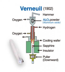
| Verneuil Method (Flame Fusion) | High-purity Al₂O₃ powder is melted in an oxyhydrogen flame, droplets solidify layer by layer on a seed | Low cost, high efficiency, relatively simple process | Gem-quality sapphires, early optical materials |
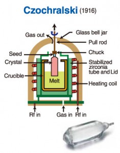
| Czochralski Method (CZ) | Al₂O₃ is melted in a crucible, and a seed crystal is slowly pulled upward to grow the crystal | Produces relatively large crystals with good integrity | Laser crystals, optical windows |
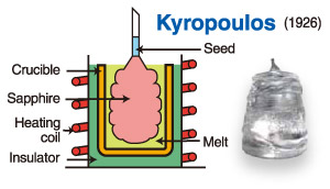
| Kyropoulos Method (KY) | Controlled slow cooling allows the crystal to grow gradually inside the crucible | Capable of growing large-size, low-stress crystals (tens of kilograms or more) | LED substrates, smartphone screens, optical components |
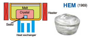
| HEM Method (Heat Exchange) | Cooling starts from the crucible top, crystals grow downward from the seed | Produces very large crystals (up to hundreds of kilograms) with uniform quality | Large optical windows, aerospace, military optics |
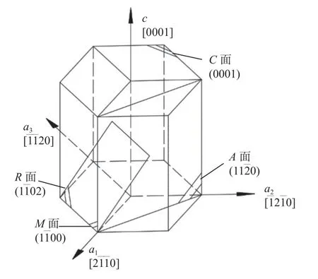
Crystal Orientation
| Orientation / Plane | Miller Index | Characteristics | Main Applications |
|---|---|---|---|
| C-plane | (0001) | Perpendicular to the c-axis, polar surface, atoms arranged uniformly | LED, laser diodes, GaN epitaxial substrates (most widely used) |
| A-plane | (11-20) | Parallel to the c-axis, non-polar surface, avoids polarization effects | Non-polar GaN epitaxy, optoelectronic devices |
| M-plane | (10-10) | Parallel to the c-axis, non-polar, high symmetry | High-performance GaN epitaxy, optoelectronic devices |
| R-plane | (1-102) | Inclined to the c-axis, excellent optical properties | Optical windows, infrared detectors, laser components |
Sapphire Wafer Specification(Customizable)
| Item | 1-inch C-plane(0001) 430μm Sapphire Wafers | |
| Crystal Materials | 99,999%, High Purity, Monocrystalline Al2O3 | |
| Grade | Prime, Epi-Ready | |
| Surface Orientation | C-plane(0001) | |
| C-plane off-angle toward M-axis 0.2 +/- 0.1° | ||
| Diameter | 25.4 mm +/- 0.1 mm | |
| Thickness | 430 μm +/- 25 μm | |
| Single Side Polished | Front Surface | Epi-polished, Ra < 0.2 nm (by AFM) |
| (SSP) | Back Surface | Fine ground, Ra = 0.8 μm to 1.2 μm |
| Double Side Polished | Front Surface | Epi-polished, Ra < 0.2 nm (by AFM) |
| (DSP) | Back Surface | Epi-polished, Ra < 0.2 nm (by AFM) |
| TTV | < 5 μm | |
| BOW | < 5 μm | |
| WARP | < 5 μm | |
| Cleaning / Packaging | Class 100 cleanroom cleaning and vacuum packaging, | |
| 25 pieces in one cassette packaging or single piece packaging. | ||
| Item | 2-inch C-plane(0001) 430μm Sapphire Wafers | |
| Crystal Materials | 99,999%, High Purity, Monocrystalline Al2O3 | |
| Grade | Prime, Epi-Ready | |
| Surface Orientation | C-plane(0001) | |
| C-plane off-angle toward M-axis 0.2 +/- 0.1° | ||
| Diameter | 50.8 mm +/- 0.1 mm | |
| Thickness | 430 μm +/- 25 μm | |
| Primary Flat Orientation | A-plane(11-20) +/- 0.2° | |
| Primary Flat Length | 16.0 mm +/- 1.0 mm | |
| Single Side Polished | Front Surface | Epi-polished, Ra < 0.2 nm (by AFM) |
| (SSP) | Back Surface | Fine ground, Ra = 0.8 μm to 1.2 μm |
| Double Side Polished | Front Surface | Epi-polished, Ra < 0.2 nm (by AFM) |
| (DSP) | Back Surface | Epi-polished, Ra < 0.2 nm (by AFM) |
| TTV | < 10 μm | |
| BOW | < 10 μm | |
| WARP | < 10 μm | |
| Cleaning / Packaging | Class 100 cleanroom cleaning and vacuum packaging, | |
| 25 pieces in one cassette packaging or single piece packaging. | ||
| Item | 3-inch C-plane(0001) 500μm Sapphire Wafers | |
| Crystal Materials | 99,999%, High Purity, Monocrystalline Al2O3 | |
| Grade | Prime, Epi-Ready | |
| Surface Orientation | C-plane(0001) | |
| C-plane off-angle toward M-axis 0.2 +/- 0.1° | ||
| Diameter | 76.2 mm +/- 0.1 mm | |
| Thickness | 500 μm +/- 25 μm | |
| Primary Flat Orientation | A-plane(11-20) +/- 0.2° | |
| Primary Flat Length | 22.0 mm +/- 1.0 mm | |
| Single Side Polished | Front Surface | Epi-polished, Ra < 0.2 nm (by AFM) |
| (SSP) | Back Surface | Fine ground, Ra = 0.8 μm to 1.2 μm |
| Double Side Polished | Front Surface | Epi-polished, Ra < 0.2 nm (by AFM) |
| (DSP) | Back Surface | Epi-polished, Ra < 0.2 nm (by AFM) |
| TTV | < 15 μm | |
| BOW | < 15 μm | |
| WARP | < 15 μm | |
| Cleaning / Packaging | Class 100 cleanroom cleaning and vacuum packaging, | |
| 25 pieces in one cassette packaging or single piece packaging. | ||
| Item | 4-inch C-plane(0001) 650μm Sapphire Wafers | |
| Crystal Materials | 99,999%, High Purity, Monocrystalline Al2O3 | |
| Grade | Prime, Epi-Ready | |
| Surface Orientation | C-plane(0001) | |
| C-plane off-angle toward M-axis 0.2 +/- 0.1° | ||
| Diameter | 100.0 mm +/- 0.1 mm | |
| Thickness | 650 μm +/- 25 μm | |
| Primary Flat Orientation | A-plane(11-20) +/- 0.2° | |
| Primary Flat Length | 30.0 mm +/- 1.0 mm | |
| Single Side Polished | Front Surface | Epi-polished, Ra < 0.2 nm (by AFM) |
| (SSP) | Back Surface | Fine ground, Ra = 0.8 μm to 1.2 μm |
| Double Side Polished | Front Surface | Epi-polished, Ra < 0.2 nm (by AFM) |
| (DSP) | Back Surface | Epi-polished, Ra < 0.2 nm (by AFM) |
| TTV | < 20 μm | |
| BOW | < 20 μm | |
| WARP | < 20 μm | |
| Cleaning / Packaging | Class 100 cleanroom cleaning and vacuum packaging, | |
| 25 pieces in one cassette packaging or single piece packaging. | ||
| Item | 6-inch C-plane(0001) 1300μm Sapphire Wafers | |
| Crystal Materials | 99,999%, High Purity, Monocrystalline Al2O3 | |
| Grade | Prime, Epi-Ready | |
| Surface Orientation | C-plane(0001) | |
| C-plane off-angle toward M-axis 0.2 +/- 0.1° | ||
| Diameter | 150.0 mm +/- 0.2 mm | |
| Thickness | 1300 μm +/- 25 μm | |
| Primary Flat Orientation | A-plane(11-20) +/- 0.2° | |
| Primary Flat Length | 47.0 mm +/- 1.0 mm | |
| Single Side Polished | Front Surface | Epi-polished, Ra < 0.2 nm (by AFM) |
| (SSP) | Back Surface | Fine ground, Ra = 0.8 μm to 1.2 μm |
| Double Side Polished | Front Surface | Epi-polished, Ra < 0.2 nm (by AFM) |
| (DSP) | Back Surface | Epi-polished, Ra < 0.2 nm (by AFM) |
| TTV | < 25 μm | |
| BOW | < 25 μm | |
| WARP | < 25 μm | |
| Cleaning / Packaging | Class 100 cleanroom cleaning and vacuum packaging, | |
| 25 pieces in one cassette packaging or single piece packaging. | ||
| Item | 8-inch C-plane(0001) 1300μm Sapphire Wafers | |
| Crystal Materials | 99,999%, High Purity, Monocrystalline Al2O3 | |
| Grade | Prime, Epi-Ready | |
| Surface Orientation | C-plane(0001) | |
| C-plane off-angle toward M-axis 0.2 +/- 0.1° | ||
| Diameter | 200.0 mm +/- 0.2 mm | |
| Thickness | 1300 μm +/- 25 μm | |
| Single Side Polished | Front Surface | Epi-polished, Ra < 0.2 nm (by AFM) |
| (SSP) | Back Surface | Fine ground, Ra = 0.8 μm to 1.2 μm |
| Double Side Polished | Front Surface | Epi-polished, Ra < 0.2 nm (by AFM) |
| (DSP) | Back Surface | Epi-polished, Ra < 0.2 nm (by AFM) |
| TTV | < 30 μm | |
| BOW | < 30 μm | |
| WARP | < 30 μm | |
| Cleaning / Packaging | Class 100 cleanroom cleaning and vacuum packaging, | |
| Single piece packaging. | ||
| Item | 12-inch C-plane(0001) 1300μm Sapphire Wafers | |
| Crystal Materials | 99,999%, High Purity, Monocrystalline Al2O3 | |
| Grade | Prime, Epi-Ready | |
| Surface Orientation | C-plane(0001) | |
| C-plane off-angle toward M-axis 0.2 +/- 0.1° | ||
| Diameter | 300.0 mm +/- 0.2 mm | |
| Thickness | 3000 μm +/- 25 μm | |
| Single Side Polished | Front Surface | Epi-polished, Ra < 0.2 nm (by AFM) |
| (SSP) | Back Surface | Fine ground, Ra = 0.8 μm to 1.2 μm |
| Double Side Polished | Front Surface | Epi-polished, Ra < 0.2 nm (by AFM) |
| (DSP) | Back Surface | Epi-polished, Ra < 0.2 nm (by AFM) |
| TTV | < 30 μm | |
| BOW | < 30 μm | |
| WARP | < 30 μm | |
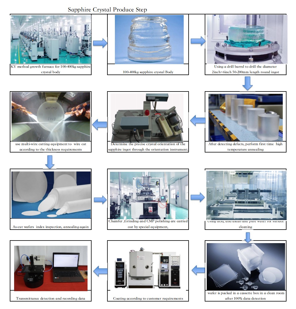
Sapphire Wafer Production Process
-
Crystal Growth
-
Grow sapphire boules (100–400 kg) using the Kyropoulos (KY) method in dedicated crystal growth furnaces.
-
-
Ingot Drilling & Shaping
-
Use a drill barrel to process the boule into cylindrical ingots with diameters of 2–6 inches and lengths of 50–200 mm.
-
-
First Annealing
-
Inspect the ingots for defects and perform the first high-temperature annealing to relieve internal stress.
-
-
Crystal Orientation
-
Determine the precise orientation of the sapphire ingot (e.g., C-plane, A-plane, R-plane) using orientation instruments.
-
-
Multi-Wire Saw Cutting
-
Slice the ingot into thin wafers according to the required thickness using multi-wire cutting equipment.
-
-
Initial Inspection & Second Annealing
-
Inspect the as-cut wafers (thickness, flatness, surface defects).
-
Conduct annealing again if necessary to further improve crystal quality.
-
-
Chamfering, Grinding & CMP Polishing
-
Perform chamfering, surface grinding, and chemical mechanical polishing (CMP) with specialized equipment to achieve mirror-grade surfaces.
-
-
Cleaning
-
Clean wafers thoroughly using ultra-pure water and chemicals in a cleanroom environment to remove particles and contaminants.
-
-
Optical & Physical Inspection
-
Conduct transmittance detection and record optical data.
-
Measure wafer parameters including TTV (Total Thickness Variation), Bow, Warp, orientation accuracy, and surface roughness.
-
-
Coating (Optional)
-
Apply coatings (e.g., AR coatings, protective layers) according to customer specifications.
-
Final Inspection & Packaging
-
Perform 100% quality inspection in a cleanroom.
-
Pack wafers in cassette boxes under Class-100 clean conditions and vacuum seal them before shipment.
Applications of Sapphire Wafers
Sapphire wafers, with their exceptional hardness, outstanding optical transmittance, excellent thermal performance, and electrical insulation, are widely applied across multiple industries. Their applications not only cover traditional LED and optoelectronic industries but are also expanding into semiconductors, consumer electronics, and advanced aerospace and defense fields.
1. Semiconductors and Optoelectronics
LED Substrates
Sapphire wafers are the primary substrates for gallium nitride (GaN) epitaxial growth, widely used in blue LEDs, white LEDs, and Mini/Micro LED technologies.
Laser Diodes (LDs)
As substrates for GaN-based laser diodes, sapphire wafers support the development of high-power, long-lifetime laser devices.
Photodetectors
In ultraviolet and infrared photodetectors, sapphire wafers are often used as transparent windows and insulating substrates.
2. Semiconductor Devices
RFICs (Radio Frequency Integrated Circuits)
Thanks to their excellent electrical insulation, sapphire wafers are ideal substrates for high-frequency and high-power microwave devices.
Silicon-on-Sapphire (SoS) Technology
By applying SoS technology, parasitic capacitance can be greatly reduced, enhancing circuit performance. This is widely used in RF communications and aerospace electronics.
3. Optical Applications
Infrared Optical Windows
With high transmittance in the 200 nm–5000 nm wavelength range, sapphire is extensively used in infrared detectors and infrared guidance systems.
High-Power Laser Windows
The hardness and thermal resistance of sapphire make it an excellent material for protective windows and lenses in high-power laser systems.
4. Consumer Electronics
Camera Lens Covers
The high hardness of sapphire ensures scratch resistance for smartphone and camera lenses.
Fingerprint Sensors
Sapphire wafers can serve as durable, transparent covers that improve accuracy and reliability in fingerprint recognition.
Smartwatches and Premium Displays
Sapphire screens combine scratch resistance with high optical clarity, making them popular in high-end electronic products.
5. Aerospace and Defense
Missile Infrared Domes
Sapphire windows remain transparent and stable under high-temperature, high-speed conditions.
Aerospace Optical Systems
They are used in high-strength optical windows and observation equipment designed for extreme environments.

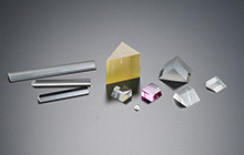
Other Common Sapphire Products
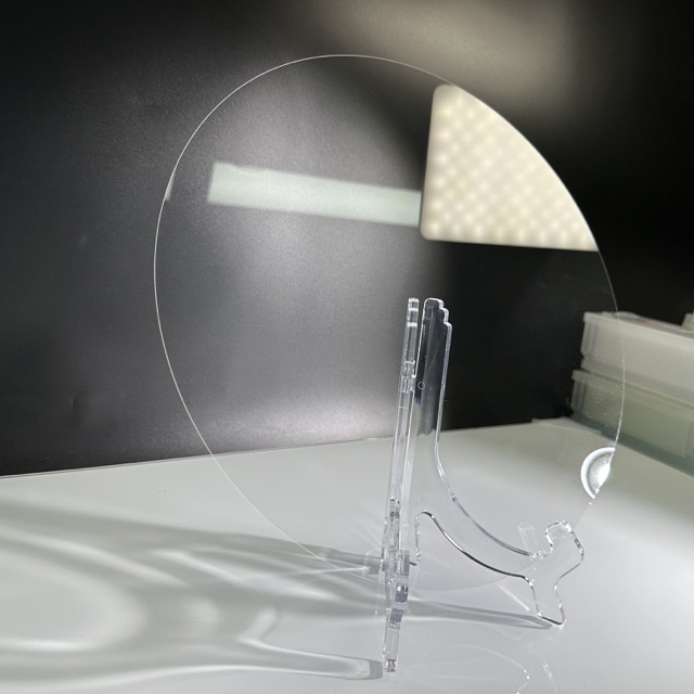
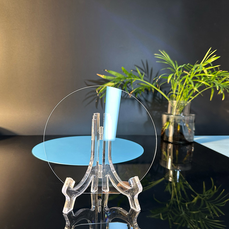
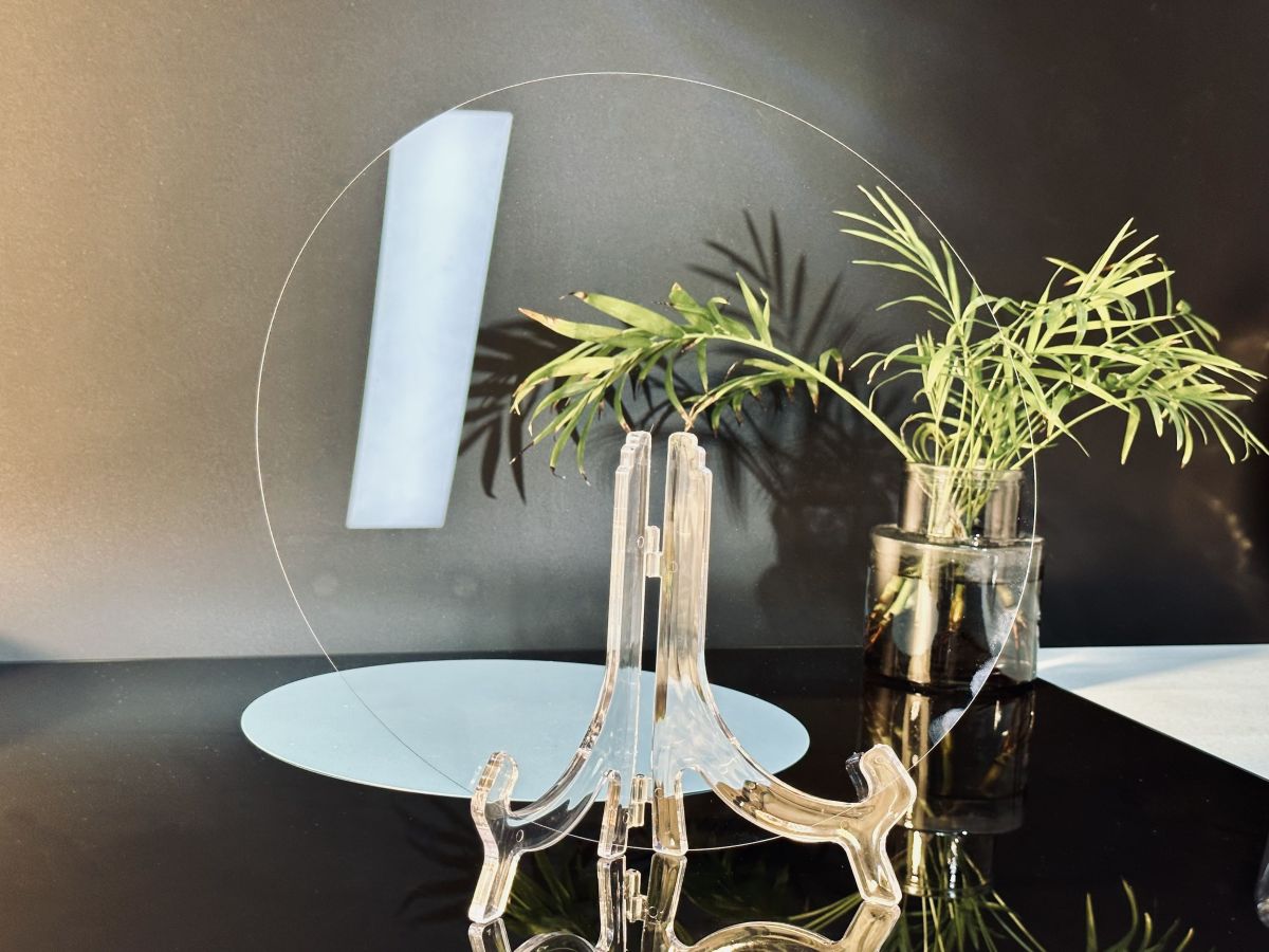
Optical Products
-
Sapphire Optical Windows
-
Used in lasers, spectrometers, infrared imaging systems, and sensor windows.
-
Transmission range: UV 150 nm to mid-IR 5.5 μm.
-
-
Sapphire Lenses
-
Applied in high-power laser systems and aerospace optics.
-
Can be manufactured as convex, concave, or cylindrical lenses.
-
-
Sapphire Prisms
-
Used in optical measurement instruments and precision imaging systems.
-
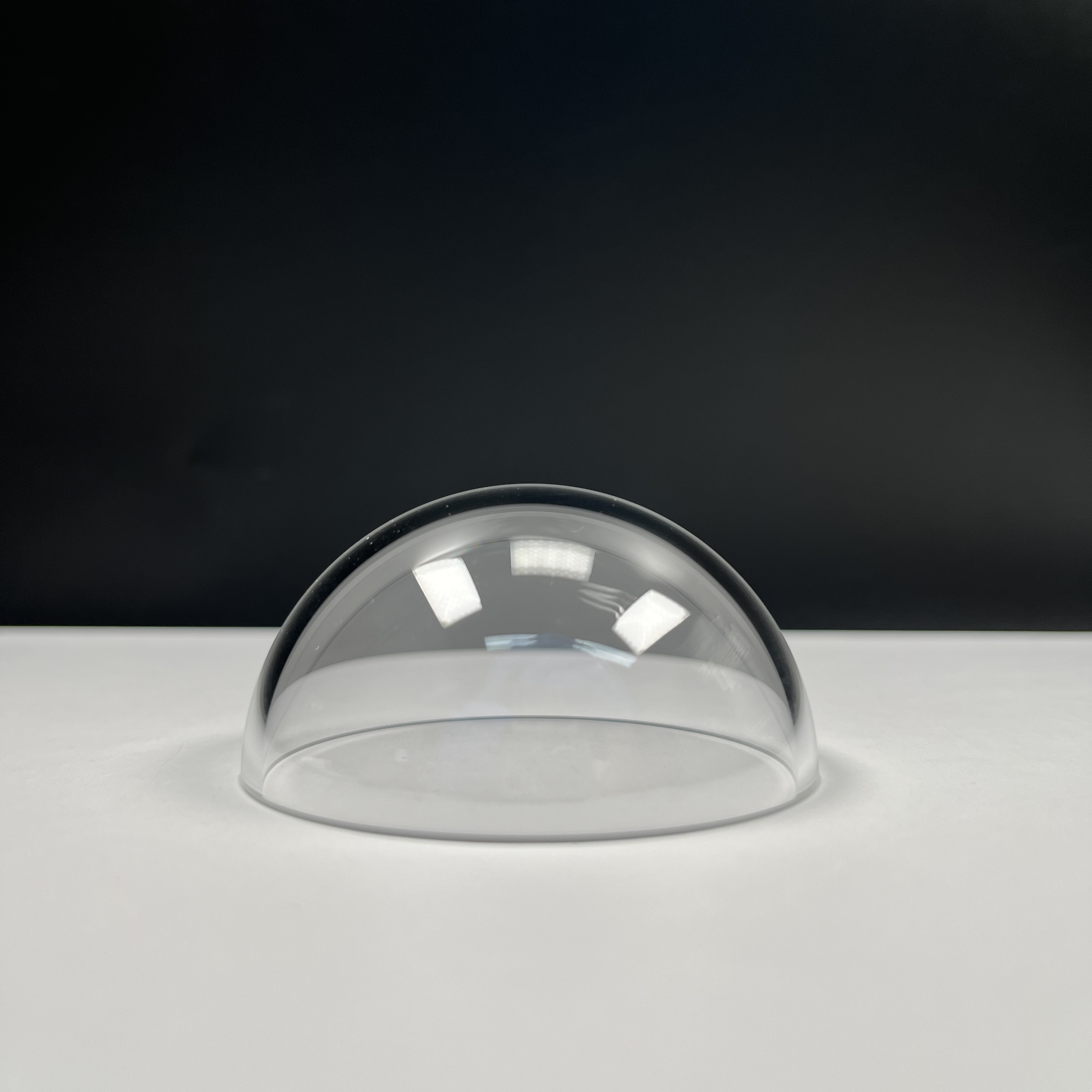
Aerospace & Defense
-
Sapphire Domes
-
Protect infrared seekers in missiles, UAVs, and aircraft.
-
-
Sapphire Protective Covers
-
Withstand high-speed airflow impact and harsh environments.
-
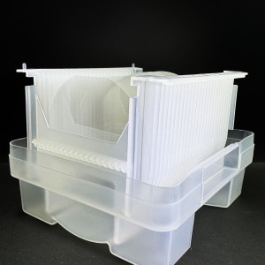
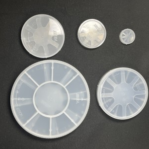
Product Packaging
About XINKEHUI
Shanghai Xinkehui New Material Co., Ltd. is one of the largest optical &semiconductor supplier in China, founded in 2002. XKH was developed to provide academic researchers with wafers and other semiconductor related scientific materials and services. Semiconductor materials is our main core business, our team is technicality based, since it's establishment, XKH is deeply involved in the research and development of advanced electronic materials, especially in the field of various wafer / substrate.

Partners
With its excellent semiconductor material technology, Shanghai Zhimingxin has become a trusted partner of the world's top companies and well-known academic institutions. With its persistence in innovation and excellence, Zhimingxin has established deep cooperative relationships with industry leaders such as Schott Glass, Corning, and Seoul Semiconductor. These collaborations have not only improved the technical level of our products, but also promoted technological development in the fields of power electronics, optoelectronic devices, and semiconductor devices.
In addition to cooperation with well-known companies, Zhimingxin has also established long-term research cooperation relationships with top universities around the world such as Harvard University, University College London (UCL), and the University of Houston. Through these collaborations, Zhimingxin not only provides technical support for scientific research projects in academia, but also participates in the development of new materials and technological innovation, ensuring that we are always at the forefront of the semiconductor industry.
Through close cooperation with these world-renowned companies and academic institutions, Shanghai Zhimingxin continues to promote technological innovation and development, providing world-class products and solutions to meet the growing needs of the global market.