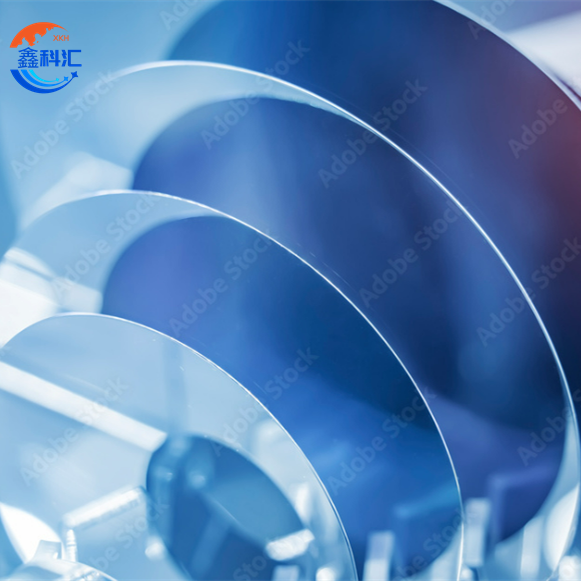
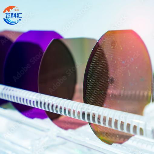
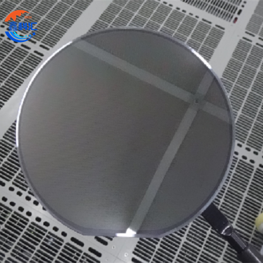
HPSI SiCOI wafer 4 6inch Hydropholic Bonding


SiCOI Wafer (Silicon Carbide-on-Insulator) Properties Overview
SiCOI wafers are a new-generation semiconductor substrate combining Silicon Carbide (SiC) with an insulating layer, often SiO₂ or sapphire, to improve performance in power electronics, RF, and photonics. Below is a detailed overview of their properties categorized into key sections:
|
Property |
Description |
| Material Composition | Silicon Carbide (SiC) layer bonded on an insulating substrate (typically SiO₂ or sapphire) |
| Crystal Structure | Typically 4H or 6H polytypes of SiC, known for high crystal quality and uniformity |
| Electrical Properties | High breakdown electric field (~3 MV/cm), wide bandgap (~3.26 eV for 4H-SiC), low leakage current |
| Thermal Conductivity | High thermal conductivity (~300 W/m·K), enabling efficient heat dissipation |
| Dielectric Layer | Insulating layer (SiO₂ or sapphire) provides electrical isolation and reduces parasitic capacitance |
| Mechanical Properties | High hardness (~9 Mohs scale), excellent mechanical strength, and thermal stability |
| Surface Finish | Typically ultra-smooth with low defect density, suitable for device fabrication |
| Applications | Power electronics, MEMS devices, RF devices, sensors requiring high temperature and voltage tolerance |
SiCOI wafers (Silicon Carbide-on-Insulator) represent an advanced semiconductor substrate structure, consisting of a high-quality thin layer of silicon carbide (SiC) bonded onto an insulating layer, typically silicon dioxide (SiO₂) or sapphire. Silicon carbide is a wide-bandgap semiconductor known for its ability to withstand high voltages and elevated temperatures, along with excellent thermal conductivity and superior mechanical hardness, making it ideal for high-power, high-frequency, and high-temperature electronic applications.
The insulating layer in SiCOI wafers provides effective electrical isolation, significantly reducing parasitic capacitance and leakage currents between devices, thereby enhancing overall device performance and reliability. The wafer surface is precisely polished to achieve ultra-smoothness with minimal defects, meeting the stringent demands of micro- and nano-scale device fabrication.
This material structure not only improves the electrical characteristics of SiC devices but also greatly enhances thermal management and mechanical stability. As a result, SiCOI wafers are widely used in power electronics, radio frequency (RF) components, microelectromechanical systems (MEMS) sensors, and high-temperature electronics. Overall, SiCOI wafers combine the exceptional physical properties of silicon carbide with the electrical isolation benefits of an insulator layer, providing an ideal foundation for the next generation of high-performance semiconductor devices.
SiCOI wafer‘s application
Power Electronics Devices
High-voltage and high-power switches, MOSFETs, and diodes
Benefit from SiC’s wide bandgap, high breakdown voltage, and thermal stability
Reduced power losses and improved efficiency in power conversion systems
Radio Frequency (RF) Components
High-frequency transistors and amplifiers
Low parasitic capacitance due to insulating layer enhances RF performance
Suitable for 5G communication and radar systems
Microelectromechanical Systems (MEMS)
Sensors and actuators operating in harsh environments
Mechanical robustness and chemical inertness extend device lifespan
Includes pressure sensors, accelerometers, and gyroscopes
High-Temperature Electronics
Electronics for automotive, aerospace, and industrial applications
Operate reliably at elevated temperatures where silicon fails
Photonic Devices
Integration with optoelectronic components on insulator substrates
Enables on-chip photonics with improved thermal management
SiCOI wafer‘s Q&A
Q:what is SiCOI wafer
A:SiCOI wafer stands for Silicon Carbide-on-Insulator wafer. It is a type of semiconductor substrate where a thin layer of silicon carbide (SiC) is bonded onto an insulating layer, usually silicon dioxide (SiO₂) or sometimes sapphire. This structure is similar in concept to the well-known Silicon-on-Insulator (SOI) wafers but uses SiC instead of silicon.
Picture