High-Thermal-Conductivity Diamond Films for AI, RF, and Power Devices


Detailed Diagram


Product Overview
The performance ceiling of advanced chips is often limited by thermal management. As AI computing, high-frequency communication, power semiconductors, and advanced packaging continue to develop rapidly, chip power density is increasing significantly. Traditional thermal materials and heat dissipation pathways are approaching their physical limits.
Diamond thin film, with its ultra-high thermal conductivity, high hardness, excellent electrical insulation, wide bandgap, low dielectric loss, corrosion resistance, and outstanding stability, is regarded as a key material for next-generation chip thermal management and high-end functionaldevices.
Through advancedMPCVD/CVD deposition technologies, high-quality diamond thin films can be grown on substrates such as silicon, silicon carbide, sapphire, quartz, and metals. They can also be processed into self-supporting diamond membranes for wafer-level heat spreading, package-level thermal management, high-frequencydevices, optoelectronic devices, and high-power chip cooling applications.
Core Product Lines
1. Ultra-Thin Diamond-on-Silicon Thin Film
Based on mature MPCVD technology, ultra-thin polycrystalline diamond films with a thickness of less than 1 μm can be directly grown on 4-inch, 6-inch, and 8-inch silicon substrates, while maintaining excellent thermal conductivity.
This structure allows the diamond heat-spreading layer to be integrateddirectlyonto the silicon-based devicesurface during wafer-level manufacturing. It functions as a near-junction heat spreader, enabling heat to spread laterally at the moment it is generated and suppressing local temperature rise at the source.
More importantly, the diamond-on-silicon process is highlycompatible with existing silicon wafer manufacturingprocesses. It can be introduced without major changes to current production lines, providing an efficient solution for thermal challenges in RF devices, power devices, high-frequencychips, and advancedpackaging.
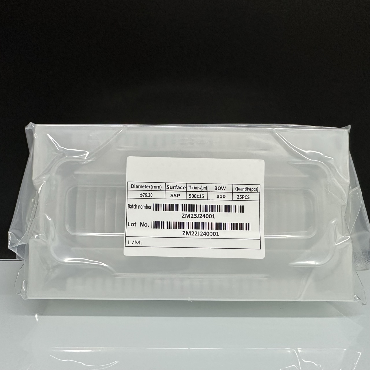
Typical Specifications
| Item | Specification |
|---|---|
| Product Type | Diamond-on-silicon thin film |
| Substrate Size | 4 inch / 6 inch / 8 inch |
| Substrate Material | Silicon |
| Diamond Type | Polycrystalline diamond thin film |
| Diamond Thickness | < 1 μm, customizable |
| Typical Thickness | 0.5 μm |
| Key Advantages | Ultra-thin, high thermal conductivity, wafer-level compatibility, near-junction heat spreading |
2. Ultra-Thin Self-Supporting Flexible Diamond Membrane
In the field of independent self-supporting diamond membranes, ultra-thin diamond films with a thickness of 5–25 μm can be produced. Compared with the commonly used 50 μm diamond membranes in the industry, this product achieves significant thickness reduction while maintaining high thermal conductivity, good thickness uniformity, and a smooth surface.
The ultra-thin self-supporting diamond membrane offers macroscopic flexibility and supports laser cutting and size customization. It eliminates the dependence on adhesive tapes or rigidcarriers and can be seamlessly integrated with advanced back-end processes such as wafer-level packaging, 3D stacking, and heterogeneous integration.
This product provides a new solution for package-level thermal management and shows strong competitiveness in flexibledevice cooling, high-frequencydevice insulation and heat conduction, optoelectronic substrates, and high-power chip thermal management.

Typical Specifications
| Item | Specification |
|---|---|
| Product Type | Self-supporting flexible diamond membrane |
| Material | CVD diamond |
| Thickness Range | 5–25 μm |
| Surface Condition | Smooth surface, customizable |
| Processing Methods | Laser cutting, size customization |
| Key Advantages | Ultra-thin, self-supporting, high thermal conductivity, flexible, suitable for advancedpackaging |
Key Features
1. Ultra-High Thermal Conductivity
Diamond is one of the best-known thermal conductive materials. Diamond thin films can rapidly spread localized heat from chips, reduce hot-spot temperature, and improve the reliability of high-power, high-frequency, and optoelectronic devices.
2. Strong Near-Junction Heat Spreading Capability
Diamond-on-silicon thin films can be directlyintegratedonto wafers or chipsurfaces, forming a near-junction heat-spreading layer. This helps conduct heat away from the heat source more efficiently and improves the limitations of conventional long thermal paths in packaging.
3. Wafer-Level Process Compatibility
4-inch, 6-inch, and 8-inch diamond-on-silicon thin films are compatible with existing silicon-based processplatforms, making them suitable for wafer-level manufacturing and scalable industrialapplications.
4. Ultra-Thin and Lightweight Structure
Diamond thin films can be fabricated at submicron thickness, while self-supporting diamond membranes can be controlled within 5–25 μm, making them suitable for miniaturized, high-density, and highlyintegrateddevices.
5. Excellent Electrical Insulation and High-Frequency Performance
Diamond offers excellent electrical insulation and low dielectric loss, making it suitable for RF devices, high-frequencychips, optoelectronic devices, and power semiconductor applications that require both insulation and thermal conductivity.
6. Outstanding Mechanical and Chemical Stability
Diamond thin films feature high hardness, wear resistance, corrosion resistance, and high-temperature stability, allowing them to maintainreliable performance in demandingenvironments.
Typical Applications
Semiconductor Thermal Management
Used for efficient heat dissipation in high-power chips, AI chips, GPUs, ASICs, GaN/SiC power devices, laser diodes, and RF devices.
Wafer-Level Heat Spreading
Diamond-on-silicon thin films can serve as wafer-level near-junction heat spreaders, enabling thermal management to be introduced during chipmanufacturing.
Advanced Packaging
Self-supporting flexible diamond membranes can be used in 2.5D/3D packaging, Chiplet integration, wafer-level packaging, and high-density heterogeneous integration for package-level thermal management.
High-Frequency and RF Devices
Suitable for RF front-end devices, high-frequency communication components, and millimeter-wave devicesrequiring low loss, high insulation, and high thermal conductivity.
Optoelectronic Devices and Lasers
Can be used as heat-spreading substrates or thermal managementlayers for laser diodes, optical communication devices, photodetectors, and high-power photonic chips.
Flexible Electronics
Ultra-thin self-supporting diamond membranes with macroscopic flexibility can be applied in flexibledevice cooling and next-generation flexibleelectronic systems.

Customizable Specifications
| Item | AvailableOptions |
|---|---|
| Material | CVD / MPCVD diamond thin film |
| Product Type | Diamond-on-silicon thin film, self-supporting diamond membrane, polycrystalline diamond film, nanocrystalline diamond film |
| Substrate Material | Si, SiC, sapphire, quartz, Mo, W, and others |
| Substrate Size | 4 inch / 6 inch / 8 inch or customized |
| Film Thickness | < 1 μm, 5–25 μm, or customized |
| Surface Condition | As-grown, polished, smooth surface |
| ProcessingServices | Cutting, polishing, laserprocessing, size customization |
| Application Fields | Wafer-level thermal management, package-level cooling, high-frequencydevices, power devices, optoelectronic devices |
FAQ
Q1: What is diamond thin film?
Diamond thin film is a high-performance functional film prepared by CVD or MPCVD technology. It combines ultra-high thermal conductivity, excellent electrical insulation, high hardness, low dielectric loss, and strong chemical stability, making it suitable for semiconductor thermal management, advancedpackaging, RF devices, power devices, and optoelectronic applications.
Q2: What are the main product types available?
The main product types include diamond-on-silicon thin films and self-supporting diamond membranes. Diamond-on-silicon films are typically used for wafer-level near-junction heat spreading, while self-supporting diamond membranes are suitable for package-level thermal management and advancedpackagingintegration.
Q3: What sizes are available for diamond-on-silicon thin films?
Diamond-on-silicon thin films can be supplied on 4-inch, 6-inch, and 8-inch silicon substrates. The diamond layer thickness can be less than 1 μm, with typical 0.5 μm.
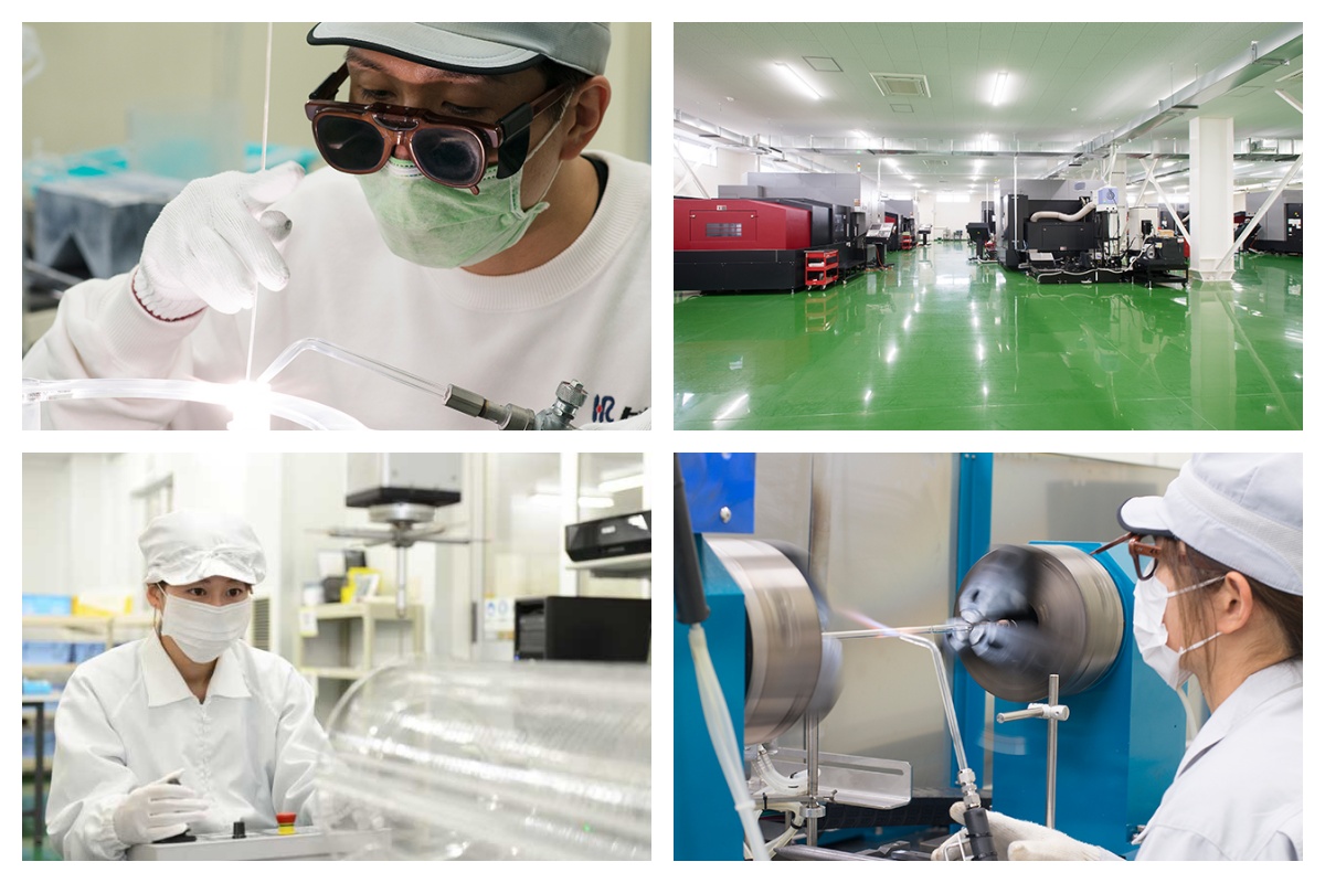
About Us
XKH specializes in high-tech development, production, and sales of special optical glass and new crystal materials. Our products serve optical electronics, consumer electronics, and the military. We offer Sapphire optical components, mobile phone lens covers, Ceramics, LT, Silicon Carbide SIC, Quartz, and semiconductor crystal wafers. With skilled expertise and cutting-edge equipment, we excel in non-standard product processing, aiming to be a leading optoelectronic materials high-tech enterprise.