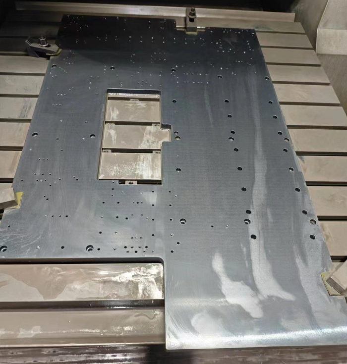
SiC Ceramic Tray End Effector Wafer Handling Custom-Made Components


SiC Ceramic & Alumina Ceramic Custom Components Brief
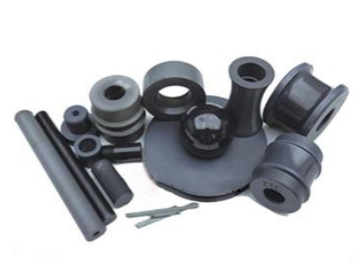
Silicon Carbide (SiC) Ceramic Custom Components
Silicon Carbide (SiC) ceramic custom components are high-performance industrial ceramic materials renowned for their extremely high hardness, excellent thermal stability, exceptional corrosion resistance, and high thermal conductivity. Silicon Carbide (SiC) ceramic custom components enable to maintain structural stability in high-temperature environments while resisting erosion from strong acids, alkalis, and molten metals. SiC ceramics are manufactured through processes such as pressureless sintering, reaction sintering, or hot-press sintering and can be customized into complex shapes, including mechanical seal rings, shaft sleeves, nozzles, furnace tubes, wafer boats, and wear-resistant lining plates.
Alumina Ceramic Custom Components
Alumina (Al₂O₃) ceramic custom components emphasize high insulation, good mechanical strength, and wear resistance. Classified by purity grades (e.g., 95%, 99%), Alumina (Al₂O₃) ceramic custom components with precision machining allows them to be crafted into insulators, bearings, cutting tools, and medical implants. Alumina ceramics are primarily manufactured via dry pressing, injection molding, or isostatic pressing processes, with surfaces polishable to a mirror finish.
XKH specializes in the R&D and custom production of silicon carbide (SiC) and alumina (Al₂O₃) ceramics. SiC ceramic products focus on high-temperature, high-wear, and corrosive environments, covering semiconductor applications (e.g., wafer boats, cantilever paddles, furnace tubes) as well as thermal field components and high-end seals for new energy sectors. Alumina ceramic products emphasize insulation, sealing, and biomedical properties, including electronic substrates, mechanical seal rings, and medical implants. Utilizing technologies such as isostatic pressing, pressureless sintering, and precision machining, we provide high-performance customized solutions for industries including semiconductors, photovoltaics, aerospace, medical, and chemical processing, ensuring components meet stringent requirements for precision, longevity, and reliability in extreme conditions.
SiC Ceramic Functional Chucks & CMP Grinding Discs Introduction
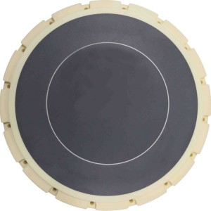
SiC Ceramic Vacuum Chucks
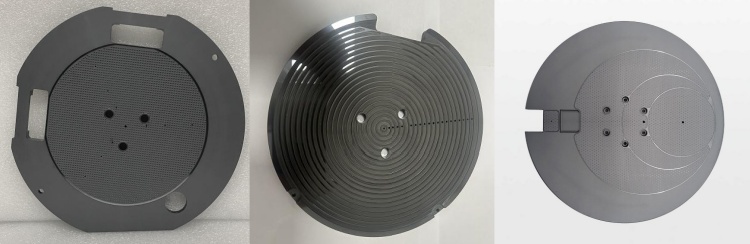
Silicon Carbide (SiC) Ceramic Vacuum Chucks are high-precision adsorption tools manufactured from high-performance silicon carbide (SiC) ceramic material. They are specifically designed for applications demanding extreme cleanliness and stability, such as semiconductor, photovoltaic, and precision manufacturing industries . Their core advantages include: a mirror-level polished surface (flatness controlled within 0.3–0.5 μm), ultra-high stiffness and low coefficient of thermal expansion (ensuring nano-level shape and position stability), an extremely lightweight structure (significantly reducing motion inertia), and exceptional wear resistance (Mohs hardness up to 9.5, far exceeding the lifespan of metal chucks) . These properties enable stable operation in environments with alternating high and low temperatures, strong corrosion, and high-speed handling, substantially improving the processing yield and production efficiency for precision components like wafers and optical elements.
Silicon Carbide (SiC) Bump Vacuum Chuck for Metrology and Inspection
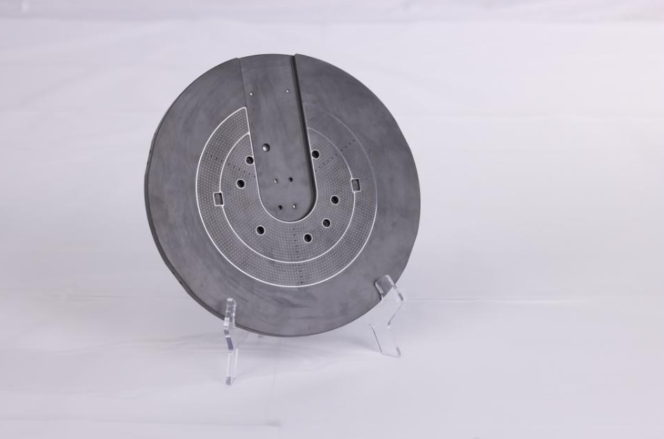
Designed for wafer defect inspection processes, this high-precision adsorption tool is manufactured from silicon carbide (SiC) ceramic material. Its unique surface bump structure provides powerful vacuum adsorption force while minimizing contact area with the wafer, thereby preventing damage or contamination to the wafer surface and ensuring stability and accuracy during inspection. The chuck features exceptional flatness (0.3–0.5 μm) and a mirror-polished surface, combined with ultra-light weight and high stiffness to ensure stability during high-speed motion. Its extremely low coefficient of thermal expansion guarantees dimensional stability under temperature fluctuations, while outstanding wear resistance extends service life. The product supports customization in 6, 8, and 12-inch specifications to meet the inspection needs of different wafer sizes.
Flip Chip Bonding Chuck
The flip chip bonding chuck is a core component in chip flip-chip bonding processes, specifically designed for precisely adsorbing wafers to ensure stability during high-speed, high-precision bonding operations. It features a mirror-polished surface (flatness/parallelism ≤1 μm) and precision gas channel grooves to achieve uniform vacuum adsorption force, preventing wafer displacement or damage. Its high stiffness and ultra-low coefficient of thermal expansion (close to silicon material) ensure dimensional stability in high-temperature bonding environments, while the high-density material (e.g., silicon carbide or specialty ceramics) effectively prevents gas permeation, maintaining long-term vacuum reliability. These characteristics collectively support micron-level bonding accuracy and significantly enhance chip packaging yield.
SiC Bonding Chuck

The silicon carbide (SiC) bonding chuck is a core fixture in chip bonding processes, specifically designed for precisely adsorbing and securing wafers, ensuring ultra-stable performance under high-temperature and high-pressure bonding conditions. Manufactured from high-density silicon carbide ceramic (porosity <0.1%), it achieves uniform adsorption force distribution (deviation <5%) through nanometer-level mirror polishing (surface roughness Ra <0.1 μm) and precision gas channel grooves (pore diameter: 5-50 μm), preventing wafer displacement or surface damage. Its ultra-low coefficient of thermal expansion (4.5×10⁻⁶/℃) closely matches that of silicon wafers, minimizing thermal stress-induced warpage. Combined with high stiffness (elastic modulus >400 GPa) and ≤1 μm flatness/parallelism, it guarantees bonding alignment accuracy. Widely used in semiconductor packaging, 3D stacking, and Chiplet integration, it supports high-end manufacturing applications requiring nanoscale precision and thermal stability.
CMP Grinding Disc
The CMP grinding disc is a core component of chemical mechanical polishing (CMP) equipment, specifically designed to securely hold and stabilize wafers during high-speed polishing, enabling nanometer-level global planarization. Constructed from high-stiffness, high-density materials (e.g., silicon carbide ceramics or specialty alloys), it ensures uniform vacuum adsorption through precision-engineered gas channel grooves. Its mirror-polished surface (flatness/parallelism ≤3 μm) guarantees stress-free contact with wafers, while an ultra-low coefficient of thermal expansion (matched to silicon) and internal cooling channels effectively suppress thermal deformation. Compatible with 12-inch (750 mm diameter) wafers, the disc leverages diffusion bonding technology to ensure seamless integration and long-term reliability of multilayer structures under high temperatures and pressures, significantly enhancing CMP process uniformity and yield.
Customized various SiC Ceramics Parts Introduction
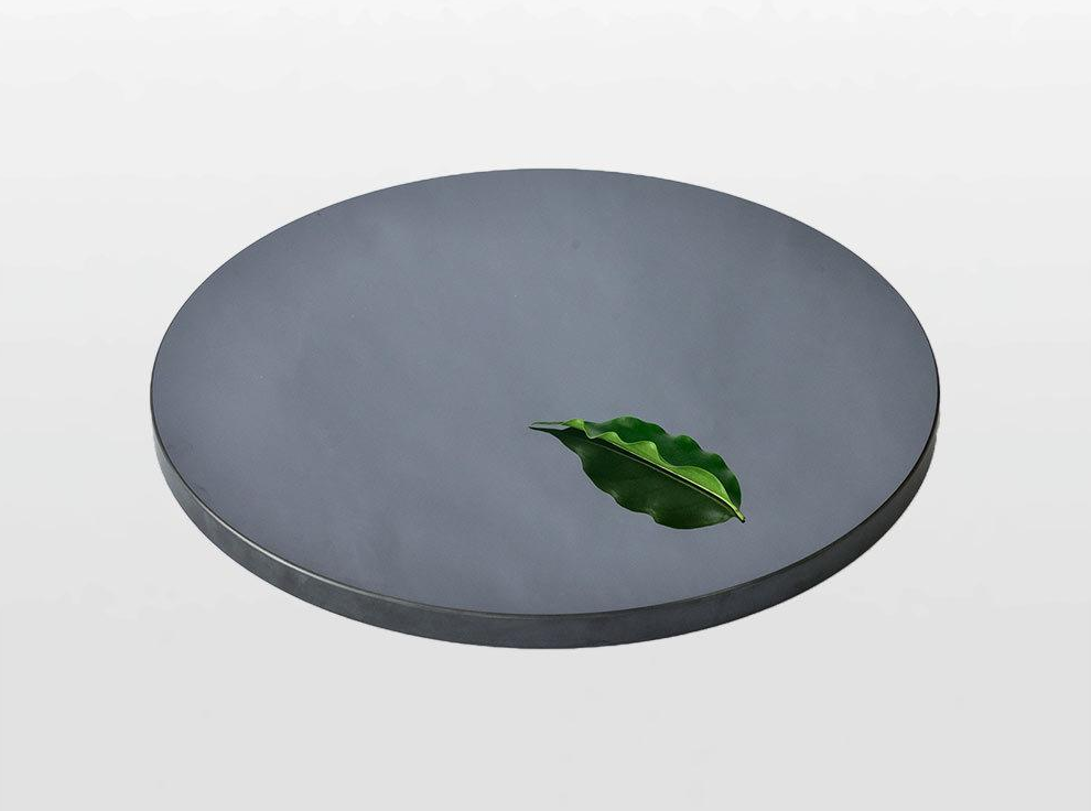
Silicon Carbide (SiC) Square Mirror
Silicon Carbide (SiC) Square Mirror is a high-precision optical component manufactured from advanced silicon carbide ceramic, specifically designed for high-end semiconductor manufacturing equipment such as lithography machines. It achieves ultra-light weight and high stiffness (elastic modulus >400 GPa) through rational lightweight structural design (e.g., backside honeycomb hollowing), while its extremely low thermal expansion coefficient (≈4.5×10⁻⁶/℃) ensures dimensional stability under temperature fluctuations. The mirror surface, after precision polishing, attains ≤1 μm flatness/parallelness, and its exceptional wear resistance (Mohs hardness 9.5) extends service life. It is widely used in lithography machine workstations, laser reflectors, and space telescopes where ultra-high precision and stability are critical.
Silicon Carbide (SiC) Air Floatation Guides
 Silicon Carbide (SiC) Air Floatation Guides utilize non-contact aerostatic bearing technology, where compressed gas forms a micron-level air film (typically 3-20μm) to achieve frictionless and vibration-free smooth motion. They offer nanometric motion accuracy (repeated positioning accuracy up to ±75nm) and sub-micron geometric precision (straightness ±0.1-0.5μm, flatness ≤1μm) , enabled by closed-loop feedback control with precision grating scales or laser interferometers . The core silicon carbide ceramic material (options include Coresic® SP/Marvel Sic series) provides ultra-high stiffness (elastic modulus >400 GPa) , ultra-low thermal expansion coefficient (4.0–4.5×10⁻⁶/K, matching silicon) , and high density (porosity <0.1%) . Its lightweight design (density 3.1g/cm³, second only to aluminum) reduces motion inertia, while exceptional wear resistance (Mohs hardness 9.5) and thermal stability ensure long-term reliability under high-speed (1m/s) and high-acceleration (4G) conditions. These guides are widely used in semiconductor lithography, wafer inspection, and ultra-precision machining.
Silicon Carbide (SiC) Cross-Beams
Silicon Carbide (SiC) Cross-Beams are core motion components designed for semiconductor equipment and high-end industrial applications, primarily functioning to carry wafer stages and guide them along specified trajectories for high-speed, ultra-precision motion. Utilizing high-performance silicon carbide ceramic (options include Coresic® SP or Marvel Sic series) and lightweight structural design, they achieve ultra-light weight with high stiffness (elastic modulus >400 GPa), along with an ultra-low coefficient of thermal expansion (≈4.5×10⁻⁶/℃) and high density (porosity <0.1%), ensuring nanometric stability (flatness/parallelism ≤1μm) under thermal and mechanical stresses. Their integrated properties support high-speed and high-acceleration operations (e.g., 1m/s, 4G), making them ideal for lithography machines, wafer inspection systems, and precision manufacturing, significantly enhancing motion accuracy and dynamic response efficiency.
Silicon Carbide (SiC) Motion Components
Silicon Carbide (SiC) Motion Components are critical parts designed for high-precision semiconductor motion systems, utilizing high-density SiC materials (e.g., Coresic® SP or Marvel Sic series, porosity <0.1%) and lightweight structural design to achieve ultra-light weight with high stiffness (elastic modulus >400 GPa). With an ultra-low coefficient of thermal expansion (≈4.5×10⁻⁶/℃), they ensure nanometric stability (flatness/parallelism ≤1μm) under thermal fluctuations. These integrated properties support high-speed and high-acceleration operations (e.g., 1m/s, 4G), making them ideal for lithography machines, wafer inspection systems, and precision manufacturing, significantly enhancing motion accuracy and dynamic response efficiency.
Silicon Carbide (SiC) Optical Path Plate
The Silicon Carbide (SiC) Optical Path Plate is a core base platform designed for dual-optical-path systems in wafer inspection equipment. Manufactured from high-performance silicon carbide ceramic, it achieves ultra-lightweight (density ≈3.1 g/cm³) and high stiffness (elastic modulus >400 GPa) through lightweight structural design, while featuring an ultra-low coefficient of thermal expansion (≈4.5×10⁻⁶/℃) and high density (porosity <0.1%), ensuring nanometric stability (flatness/parallelism ≤0.02mm) under thermal and mechanical fluctuations. With its large maximum size (900×900mm) and exceptional comprehensive performance, it provides a long-term stable mounting baseline for optical systems, significantly enhancing inspection accuracy and reliability. It is widely used in semiconductor metrology, optical alignment, and high-precision imaging systems.
Graphite + Tantalum Carbide Coated Guide Ring
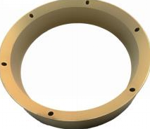
The Graphite + Tantalum Carbide Coated Guide Ring is a critical component specifically designed for silicon carbide (SiC) single crystal growth equipment. Its core function is to precisely direct high-temperature gas flow, ensuring uniformity and stability of the temperature and flow fields within the reaction chamber. Manufactured from high-purity graphite substrate (purity >99.99%) coated with a CVD-deposited tantalum carbide (TaC) layer (coating impurity content <5 ppm), it exhibits exceptional thermal conductivity (≈120 W/m·K) and chemical inertness under extreme temperatures (withstanding up to 2200°C), effectively preventing silicon vapor corrosion and suppressing impurity diffusion. The coating's high uniformity (deviation <3%, full-area coverage) ensures consistent gas guidance and long-term service reliability, significantly enhancing the quality and yield of SiC single crystal growth.
Silicon Carbide (SiC) Furnace Tube Abstract
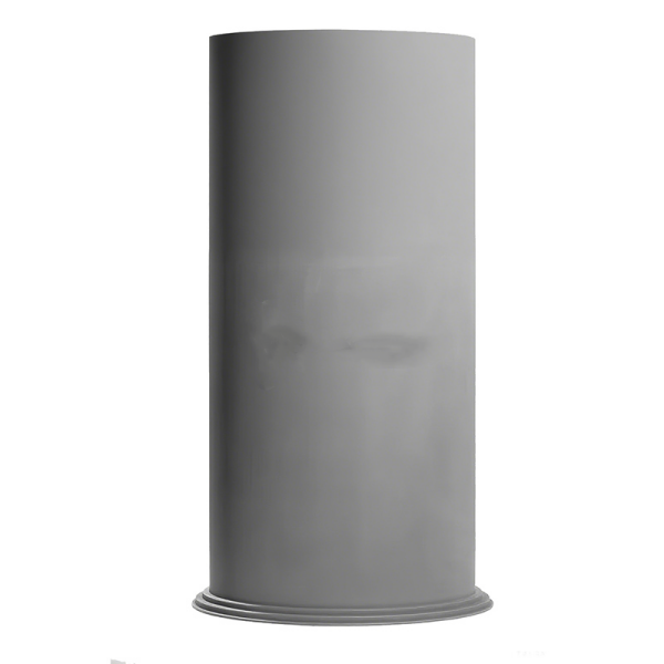
Silicon Carbide (SiC) Vertical Furnace Tube
Silicon Carbide (SiC) Vertical Furnace Tube is a critical component designed for high-temperature industrial equipment, primarily serving as an external protective tube to ensure uniform thermal distribution within the furnace under air atmosphere, with a typical operating temperature of around 1200°C. Manufactured via 3D printing integrated forming technology, it features a base material impurity content <300 ppm, and can be optionally equipped with a CVD silicon carbide coating (coating impurities <5 ppm). Combining high thermal conductivity (≈20 W/m·K) and exceptional thermal shock stability (resisting thermal gradients >800°C), it is widely used in high-temperature processes such as semiconductor heat treatment, photovoltaic material sintering, and precision ceramic production, significantly enhancing thermal uniformity and long-term reliability of equipment.
Silicon Carbide (SiC) Horizontal Furnace Tube
The Silicon Carbide (SiC) Horizontal Furnace Tube is a core component designed for high-temperature processes, serving as a process tube operating in atmospheres containing oxygen (reactive gas), nitrogen (protective gas), and trace hydrogen chloride, with a typical operating temperature of around 1250°C. Manufactured via 3D printing integrated forming technology, it features a base material impurity content <300 ppm, and can be optionally equipped with a CVD silicon carbide coating (coating impurities <5 ppm). Combining high thermal conductivity (≈20 W/m·K) and exceptional thermal shock stability (resisting thermal gradients >800°C), it is ideal for demanding semiconductor applications such as oxidation, diffusion, and thin-film deposition, ensuring structural integrity, atmosphere purity, and long-term thermal stability under extreme conditions.
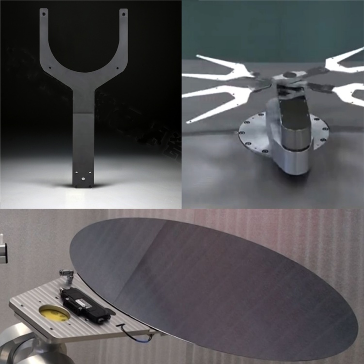
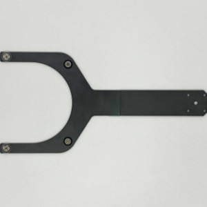
SiC Ceramic Fork Arms Introduction
Semiconductor Manufacturing
In semiconductor wafer manufacturing, SiC ceramic fork arms are primarily used for transferring and positioning wafers, commonly found in:
- Wafer Processing Equipment: Such as wafer cassettes and process boats, which operate stably in high-temperature and corrosive process environments.
- Lithography Machines: Used in precision components like stages, guides, and robotic arms, where their high rigidity and low thermal deformation ensure nanometer-level motion accuracy.
- Etching and Diffusion Processes: Serving as ICP etching trays and components for semiconductor diffusion processes, their high purity and corrosion resistance prevent contamination in process chambers.
Industrial Automation and Robotics
SiC ceramic fork arms are critical components in high-performance industrial robots and automated equipment:
- Robotic End Effectors: Used for handling, assembly, and precision operations. Their lightweight properties (density ~3.21 g/cm³) enhance robot speed and efficiency, while their high hardness (Vickers hardness ~2500) ensures exceptional wear resistance.
- Automated Production Lines: In scenarios requiring high-frequency, high-precision handling (e.g., e-commerce warehouses, factory storage), SiC fork arms guarantee long-term stable performance.
Aerospace and New Energy
In extreme environments, SiC ceramic fork arms leverage their high-temperature resistance, corrosion resistance, and thermal shock resistance:
- Aerospace: Used in critical components of spacecraft and drones, where their lightweight and high-strength properties help reduce weight and enhance performance.
- New Energy: Applied in production equipment for the photovoltaic industry (e.g., diffusion furnaces) and as precision structural components in lithium-ion battery manufacturing.
High-Temperature Industrial Processing
SiC ceramic fork arms can withstand temperatures exceeding 1600°C, making them suitable for:
- Metallurgy, Ceramics, and Glass Industries: Used in high-temperature manipulators, setter plates, and push plates.
- Nuclear Energy: Due to their radiation resistance, they are suitable for certain components in nuclear reactors.
Medical Equipment
In the medical field, SiC ceramic fork arms are primarily used for:
- Medical Robots and Surgical Instruments: Valued for their biocompatibility, corrosion resistance, and stability in sterilization environments.
SiC Coating Overview
|
Typical properties |
Units |
Values |
|
Structure |
|
FCC β phase |
|
Orientation |
Fraction (%) |
111 preferred |
|
Bulk density |
g/cm³ |
3.21 |
|
Hardness |
Vickers hardness |
2500 |
|
Heat Capacity |
J·kg-1 ·K-1 |
640 |
|
Thermal expansion 100–600 °C (212–1112 °F) |
10-6K-1 |
4.5 |
|
Young’ s Modulus |
Gpa (4pt bend, 1300℃) |
430 |
|
Grain Size |
μm |
2~10 |
|
Sublimation Temperature |
℃ |
2700 |
|
Felexural Strength |
MPa (RT 4-point) |
415 |
|
Thermal conductivity |
(W/mK) |
300 |
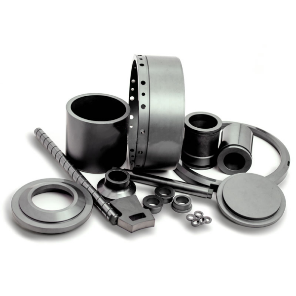
Silicon Carbide Ceramic Structural Parts Overview
 Silicon carbide ceramic structural components are obtained from silicon carbide particles bonded together through sintering. They are widely used in the automotive, machinery, chemical, semiconductor, space technology, microelectronics, and energy sectors, playing a critical role in various applications within these industries. Due to their exceptional properties, silicon carbide ceramic structural components have become an ideal material for harsh conditions involving high temperature, high pressure, corrosion, and wear, delivering reliable performance and longevity in challenging operating environments.
 SiC Seal Parts Overview
SiC seals are an ideal choice for harsh environments (such as high temperature, high pressure, corrosive media, and high-speed wear) due to their exceptional hardness, wear resistance, high-temperature resistance (withstanding temperatures up to 1600°C or even 2000°C), and corrosion resistance. Their high thermal conductivity facilitates efficient heat dissipation, while their low friction coefficient and self-lubricating properties further ensure sealing reliability and long service life under extreme operating conditions. These characteristics make SiC seals widely used in industries such as petrochemicals, mining, semiconductor manufacturing, wastewater treatment, and energy, significantly reducing maintenance costs, minimizing downtime, and enhancing equipment operational efficiency and safety.
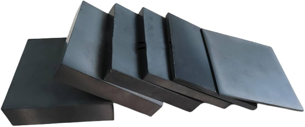
SiC Ceramic Plates Brief
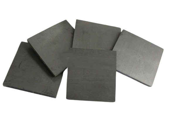
Silicon Carbide (SiC) ceramic plates are renowned for their exceptional hardness (Mohs hardness up to 9.5, second only to diamond), outstanding thermal conductivity (far exceeding most ceramics for efficient heat management), and remarkable chemical inertness and thermal shock resistance (withstanding strong acids, alkalis, and rapid temperature fluctuations). These properties ensure structural stability and reliable performance in extreme environments (e.g., high temperature, abrasion, and corrosion), while extending service life and reducing maintenance needs.
SiC ceramic plates are widely used in high-performance fields:
•Abrasives and Grinding Tools: Leveraging ultra-high hardness for manufacturing grinding wheels and polishing tools, enhancing precision and durability in abrasive environments.
•Refractory Materials: Serving as furnace linings and kiln components, maintaining stability above 1600°C to improve thermal efficiency and reduce maintenance costs.
•Semiconductor Industry: Acting as substrates for high-power electronic devices (e.g., power diodes and RF amplifiers), supporting high-voltage and high-temperature operations to boost reliability and energy efficiency.
•Casting and Smelting: Replacing traditional materials in metal processing to ensure efficient heat transfer and chemical corrosion resistance, enhancing metallurgical quality and cost-effectiveness.
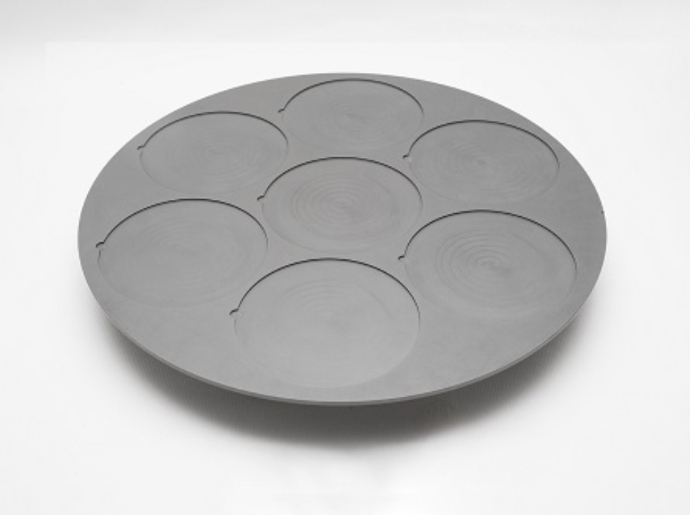
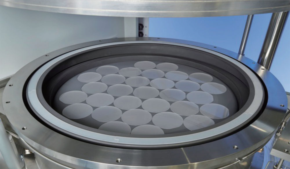
SiC Wafer Boat Abstract
XKH SiC ceramic boats deliver superior thermal stability, chemical inertness, precision engineering, and economic efficiency, providing a high-performance carrier solution for semiconductor manufacturing. They significantly enhance wafer handling safety, cleanliness, and production efficiency, making them indispensable components in advanced wafer fabrication.
SiC ceramic boats Applications:
SiC ceramic boats are widely used in front-end semiconductor processes, including:
•Deposition Processes: Such as LPCVD (Low-Pressure Chemical Vapor Deposition) and PECVD (Plasma-Enhanced Chemical Vapor Deposition).
•High-Temperature Treatments: Including thermal oxidation, annealing, diffusion, and ion implantation.
•Wet & Cleaning Processes: Wafer cleaning and chemical handling stages.
Compatible with both atmospheric and vacuum process environments,
they are ideal for fabs seeking to minimize contamination risks and improve production efficiency.
Parameters of SiC Wafer Boat:
|
Technical Properties |
||||
|
Index |
Unit |
Value |
||
|
Material Name |
Reaction Sintered Silicon Carbide |
Pressureless Sintered Silicon Carbide |
Recrystallized Silicon Carbide |
|
|
Composition |
RBSiC |
SSiC |
R-SiC |
|
|
Bulk Density |
g/cm3 |
3 |
3.15 ± 0.03 |
2.60-2.70 |
|
Flexural Strength |
MPa (kpsi) |
338(49) |
380(55) |
80-90 (20°C) 90-100(1400°C) |
|
Compressive Strength |
MPa (kpsi) |
1120(158) |
3970(560) |
> 600 |
|
Hardness |
Knoop |
2700 |
2800 |
/ |
|
Breaking Tenacity |
MPa m1/2 |
4.5 |
4 |
/ |
|
Thermal Conductivity |
W/m.k |
95 |
120 |
23 |
|
Coefficient of Thermal Expansion |
10-6.1/°C |
5 |
4 |
4.7 |
|
Specific Heat |
Joule/g 0k |
0.8 |
0.67 |
/ |
|
Max temperature in air |
℃ |
1200 |
1500 |
1600 |
|
Elastic Modulus |
Gpa |
360 |
410 |
240 |
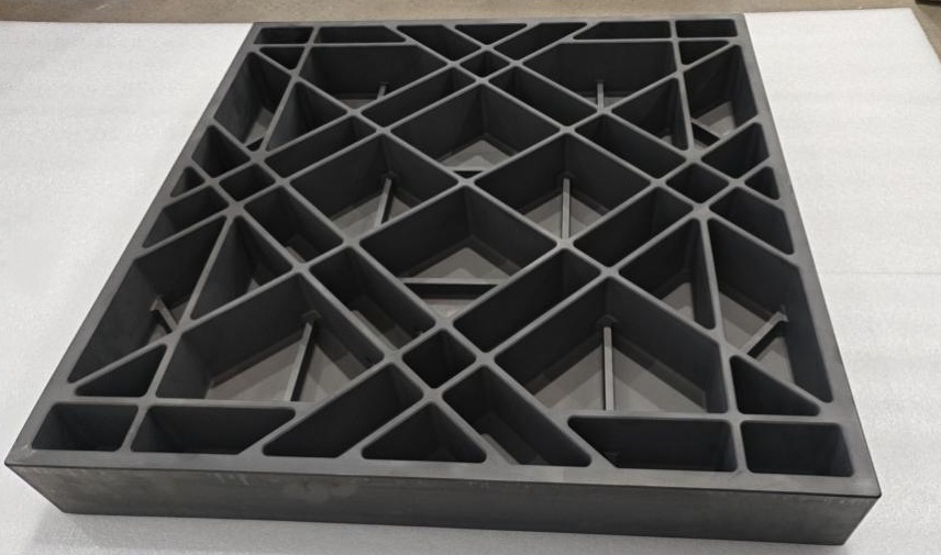
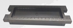
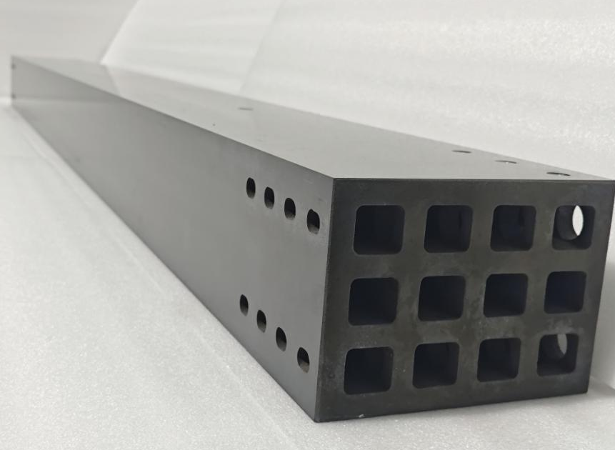
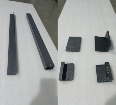
SiC Ceramics Various Custom Components Display
SiC Ceramic Membrane
SiC ceramic membrane is an advanced filtration solution crafted from pure silicon carbide, featuring a robust three-layer structure (support layer, transition layer, and separation membrane) engineered through high-temperature sintering processes. This design ensures exceptional mechanical strength, precise pore size distribution, and outstanding durability. It excels in diverse industrial applications by efficiently separating, concentrating, and purifying fluids. Key uses include water and wastewater treatment (removing suspended solids, bacteria, and organic pollutants), food and beverage processing (clarifying and concentrating juices, dairy, and fermented liquids), pharmaceutical and biotechnology operations (purifying biofluids and intermediates), chemical processing (filtering corrosive fluids and catalysts), and oil and gas applications (treating produced water and contaminant removal).
SiC Pipes
SiC (silicon carbide) tubes are high-performance ceramic components designed for semiconductor furnace systems,manufactured from high-purity fine-grained silicon carbide through advanced sintering techniques. They exhibit exceptional thermal conductivity, high-temperature stability (withstanding over 1600°C), and chemical corrosion resistance. Their low thermal expansion coefficient and high mechanical strength ensure dimensional stability under extreme thermal cycling, effectively reducing thermal stress deformation and wear. SiC tubes are suitable for diffusion furnaces, oxidation furnaces, and LPCVD/PECVD systems, enabling uniform temperature distribution and stable process conditions to minimize wafer defects and improve thin-film deposition homogeneity. Additionally, the dense, non-porous structure and chemical inertness of SiC resist erosion from reactive gases such as oxygen, hydrogen, and ammonia, extending service life and ensuring process cleanliness. SiC tubes can be customized in size and wall thickness, with precision machining achieving smooth inner surfaces and high concentricity to support laminar flow and balanced thermal profiles. Surface polishing or coating options further reduce particle generation and enhance corrosion resistance, meeting the stringent requirements of semiconductor manufacturing for precision and reliability.
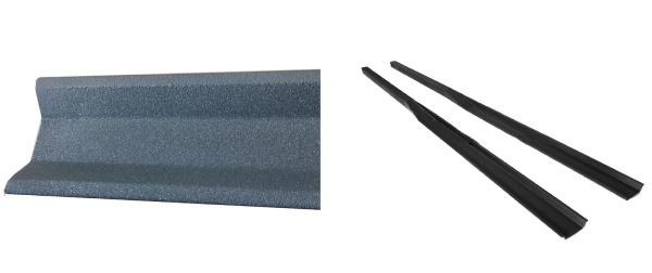
SiC Ceramic Cantilever Paddle
The monolithic design of SiC cantilever blades significantly enhances mechanical robustness and thermal uniformity while eliminating joints and weak points common in composite materials. Their surface is precision-polished to near-mirror finish, minimizing particulate generation and meeting cleanroom standards. The inherent chemical inertia of SiC prevents outgassing, corrosion, and process contamination in reactive environments (e.g., oxygen, steam), ensuring stability and reliability in diffusion/oxidation processes. Despite rapid thermal cycling, SiC maintains structural integrity, extending service life and reducing maintenance downtime. The lightweight nature of SiC enables faster thermal response, accelerating heating/cooling rates and improving productivity and energy efficiency. These blades are available in customizable sizes (compatible with 100mm to 300mm+ wafers) and adapt to various furnace designs, delivering consistent performance in both front-end and back-end semiconductor processes.
Alumina Vacuum Chuck Introduction
Al₂O₃ vacuum chucks are critical tools in semiconductor manufacturing, providing stable and precise support across multiple processes:•Thinning: Offers uniform support during wafer thinning, ensuring high-precision substrate reduction to enhance chip heat dissipation and device performance.
•Dicing: Provides secure adsorption during wafer dicing, minimizing damage risks and ensuring clean cuts for individual chips.
•Cleaning: Its smooth, uniform adsorption surface enables effective contaminant removal without damaging wafers during cleaning processes.
•Transporting: Delivers reliable and secure support during wafer handling and transportation, reducing risks of damage and contamination.
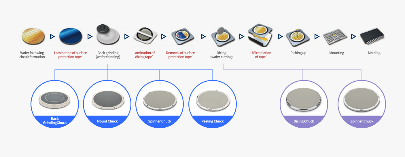
1.Uniform Micro-Porous Ceramic Technology
•Utilizes nano-powders to create evenly distributed and interconnected pores, resulting in high porosity and a uniformly dense structure for consistent and reliable wafer support.
2.Exceptional Material Properties
-Fabricated from ultra-pure 99.99% alumina (Al₂O₃), it exhibits:
•Thermal Properties: High heat resistance and excellent thermal conductivity, suitable for high-temperature semiconductor environments.
•Mechanical Properties: High strength and hardness ensure durability, wear resistance, and long service life.
•Additional Advantages: High electrical insulation and corrosion resistance, adaptable to diverse manufacturing conditions.
3.Superior Flatness and Parallelism•Ensures precise and stable wafer handling with high flatness and parallelism, minimizing damage risks and ensuring consistent processing results. Its good air permeability and uniform adsorption force further enhance operational reliability.
The Al₂O₃ vacuum chuck integrates advanced micro-porous technology, exceptional material properties, and high precision to support critical semiconductor processes, ensuring efficiency, reliability, and contamination control across thinning, dicing, cleaning, and transporting stages.
Alumina Robot Arm & Alumina Ceramic End Effector Brief
Alumina (Al₂O₃) ceramic robotic arms are critical components for wafer handling in semiconductor manufacturing. They directly contact wafers and are responsible for precise transfer and positioning in demanding environments such as vacuum or high-temperature conditions. Their core value lies in ensuring wafer safety, preventing contamination, and improving equipment operational efficiency and yield through exceptional material properties.
|
Feature Dimension |
Detailed Description |
|
Mechanical Properties |
High-purity alumina (e.g., >99%) provides high hardness (Mohs hardness up to 9) and flexural strength (up to 250-500 MPa), ensuring wear resistance and deformation avoidance, thereby extending service life.
|
|
Electrical Insulation |
Room temperature resistivity up to 10¹⁵ Ω·cm and insulation strength of 15 kV/mm effectively prevent electrostatic discharge (ESD), protecting sensitive wafers from electrical interference and damage.
|
|
Thermal Stability |
Melting point as high as 2050°C enables withstand high-temperature processes (e.g., RTA, CVD) in semiconductor manufacturing. Low thermal expansion coefficient minimizes warping and maintains dimensional stability under heat.
|
|
Chemical Inertness |
Inert to most acids, alkalis, process gases, and cleaning agents, preventing particle contamination or metal ion release. This ensures an ultra-clean production environment and avoids wafer surface contamination.
|
|
Other Advantages |
Mature processing technology offers high cost-effectiveness; surfaces can be precision-polished to low roughness, further reducing particulate generation risks.
|
Alumina ceramic robotic arms are primarily used in front-end semiconductor manufacturing processes, including:
•Wafer Handling and Positioning: Safely and precisely transfer and position wafers (e.g., 100mm to 300mm+ sizes) in vacuum or high-purity inert gas environments, minimizing damage and contamination risks.
•High-Temperature Processes: Such as rapid thermal annealing (RTA), chemical vapor deposition (CVD), and plasma etching, where they maintain stability under high temperatures, ensuring process consistency and yield.
•Automated Wafer Handling Systems: Integrated into wafer handling robots as end effectors to automate wafer transfer between equipment, enhancing production efficiency.
Conclusion
XKH specializes in the R&D and production of customized silicon carbide (SiC) and alumina (Al₂O₃) ceramic components, including robotic arms, cantilever paddles, vacuum chucks, wafer boats, furnace tubes, and other high-performance parts, serving semiconductors, new energy, aerospace, and high-temperature industries. We adhere to precision manufacturing, strict quality control, and technological innovation, leveraging advanced sintering processes (e.g., pressureless sintering, reaction sintering) and precision machining techniques (e.g., CNC grinding, polishing) to ensure exceptional high-temperature resistance, mechanical strength, chemical inertness, and dimensional accuracy. We support customization based on drawings, offering tailored solutions for dimensions, shapes, surface finishes, and material grades to meet specific client requirements. We are committed to providing reliable and efficient ceramic components for global high-end manufacturing, enhancing equipment performance and production efficiency for our customers.
Related Products
-
SiC ceramic tray plate graphite with CVD SiC co...
-

Silicon Carbide (SiC) Horizontal Furnace Tube
-

SiC ceramic chuck tray Ceramic suction cups pre...
-

High strength silicon carbide ceramic tube SIC ...
-

Industrial SiC Vertical Furnace Tube High Therm...
-
Alumina ceramic wafer 4inch purity 99% polycrys...