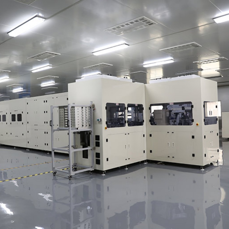
Silicon / Silicon Carbide (SiC) Wafer Four-Stage Linked Polishing Automation Line (Integrated Post-Polish Handling Line)


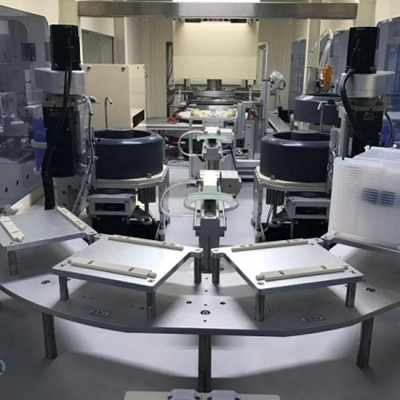
Detailed Diagram


Overview
This Four-Stage Linked Polishing Automation Line is an integrated, in-line solution designed for post-polish / post-CMP operations of silicon and silicon carbide (SiC) wafers. Built around ceramic carriers (ceramic plates), the system combines multiple downstream tasks into one coordinated line—helping fabs reduce manual handling, stabilize takt time, and strengthen contamination control.
In semiconductor manufacturing, effective post-CMP cleaning is widely recognized as a key step to reduce defects before the next process, and advanced approaches (including megasonic cleaning) are commonly discussed for improving particle removal performance.
For SiC in particular, its high hardness and chemical inertness make polishing challenging (often associated with low material removal rate and higher risk of surface/subsurface damage), which makes stable post-polish automation and controlled cleaning/handling especially valuable.
Key Benefits
A single integrated line that supports:
-
Wafer separation and collection (after polishing)
-
Ceramic carrier buffering / storage
-
Ceramic carrier cleaning
-
Wafer mounting (pasting) onto ceramic carriers
-
Consolidated, one-line operation for 6–8 inch wafers
Technical Specifications (From Provided Datasheet)
-
Equipment Dimensions (L×W×H): 13643 × 5030 × 2300 mm
-
Power Supply: AC 380 V, 50 Hz
-
Total Power: 119 kW
-
Mounting Cleanliness: 0.5 μm < 50 ea; 5 μm < 1 ea
-
Mounting Flatness: ≤ 2 μm
Throughput Reference (From Provided Datasheet)
-
Equipment Dimensions (L×W×H): 13643 × 5030 × 2300 mm
-
Power Supply: AC 380 V, 50 Hz
-
Total Power: 119 kW
-
Mounting Cleanliness: 0.5 μm < 50 ea; 5 μm < 1 ea
-
Mounting Flatness: ≤ 2 μm
Typical Line Flow
-
Infeed / interface from upstream polishing area
-
Wafer separation & collection
-
Ceramic carrier buffering/storage (takt-time decoupling)
-
Ceramic carrier cleaning
-
Wafer mounting onto carriers (with cleanliness & flatness control)
-
Outfeed to downstream process or logistics
FAQ
Q1: What problems does this line primarily solve?
A: It streamlines post-polish operations by integrating wafer separation/collection, ceramic carrier buffering, carrier cleaning, and wafer mounting into one coordinated automation line—reducing manual touchpoints and stabilizing production rhythm.
Q2: Which wafer materials and sizes are supported?
A: Silicon and SiC, 6–8 inch wafers (per the provided spec).
Q3: Why is post-CMP cleaning emphasized in the industry?
A: Industry literature highlights that demand for effective post-CMP cleaning has grown to reduce defect density before the next step; megasonic-based approaches are commonly studied for improving particle removal.
About Us
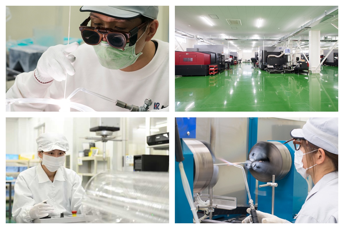
XKH specializes in high-tech development, production, and sales of special optical glass and new crystal materials. Our products serve optical electronics, consumer electronics, and the military. We offer Sapphire optical components, mobile phone lens covers, Ceramics, LT, Silicon Carbide SIC, Quartz, and semiconductor crystal wafers. With skilled expertise and cutting-edge equipment, we excel in non-standard product processing, aiming to be a leading optoelectronic materials high-tech enterprise.
Related Products
-

Lab-Created Ruby Rough Stone vivid red Internal...
-

4H-N Dia205mm SiC seed from China P and D grade...
-

GaN-on-Diamond Wafers 4inch 6inch Total epi thi...
-

Mg-Doped LiNbO₃Ingots 45°Z-Cut 64°Y-Cut Orienta...
-

InGaAs epitaxial wafer substrate PD Array photo...
-

SiC wafer 4H-N 6H-N HPSI 4H-semi 6H-semi 4H-P 6...