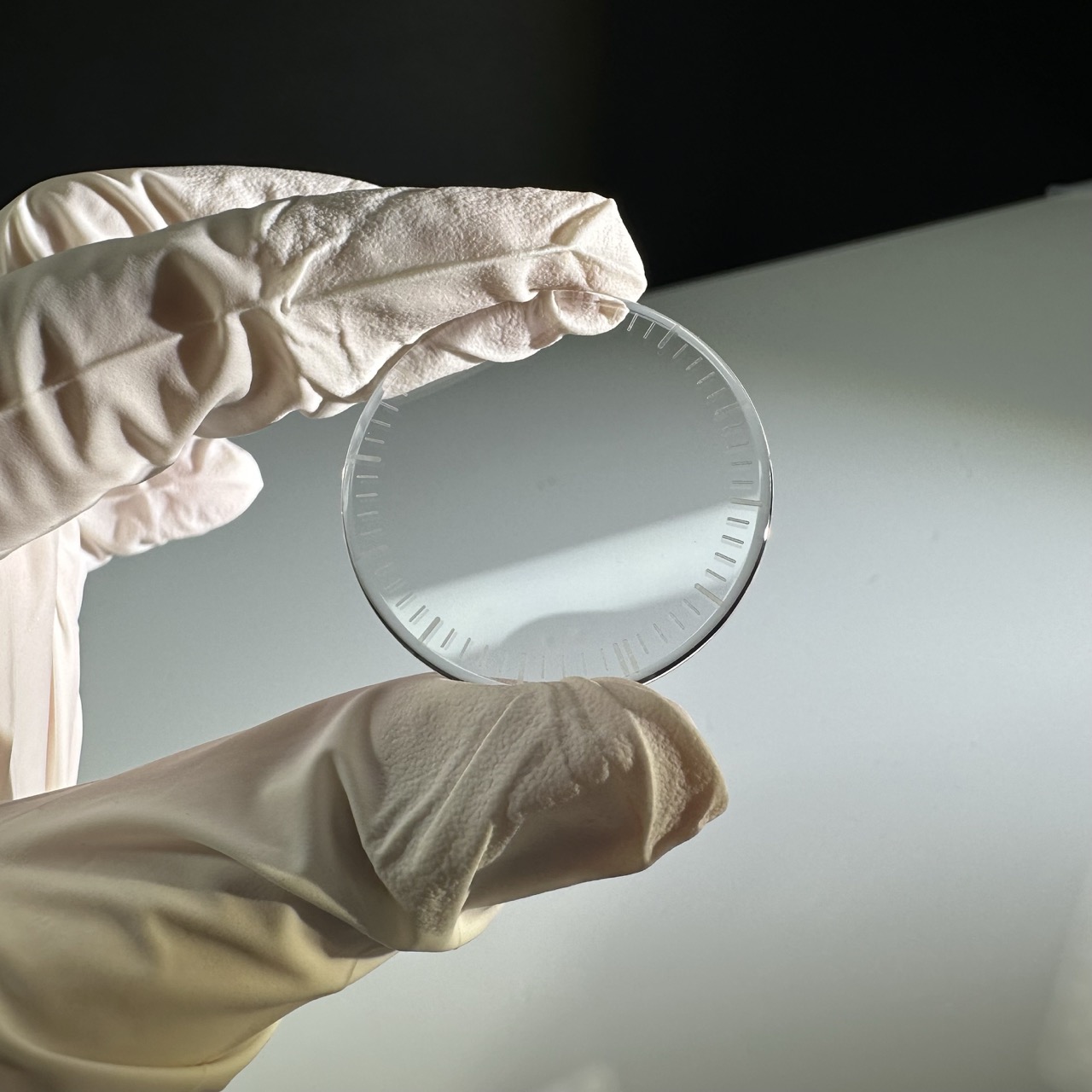
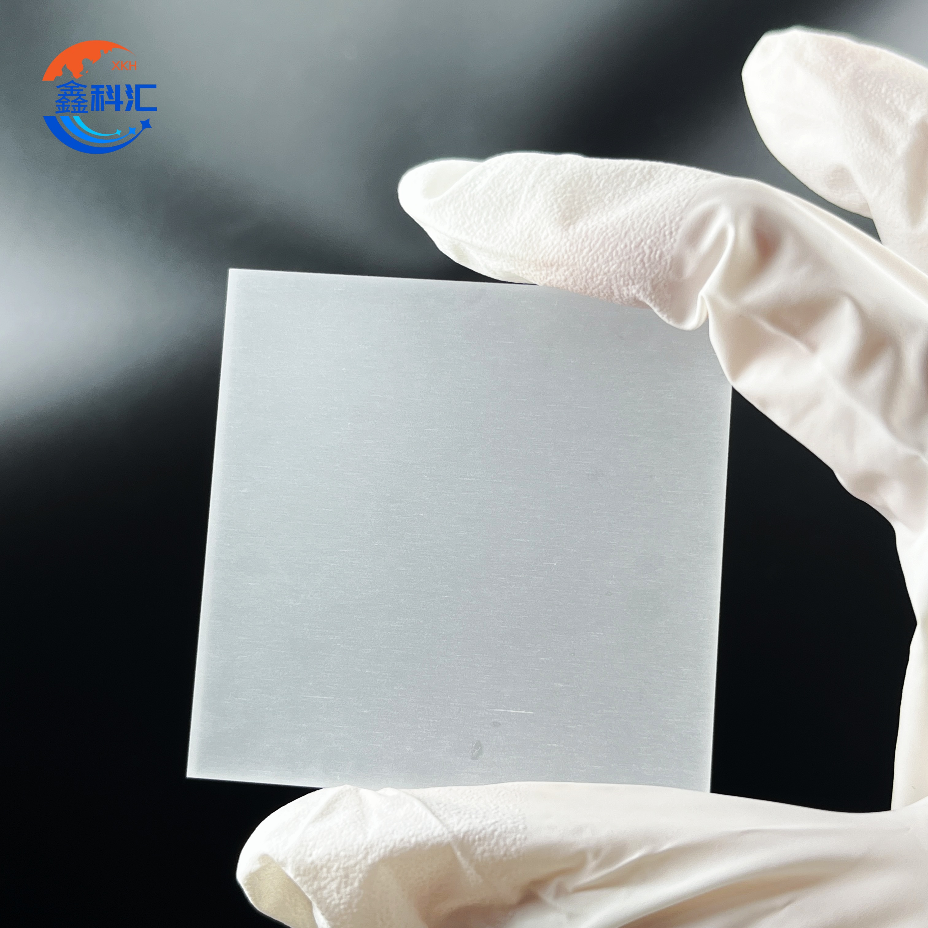
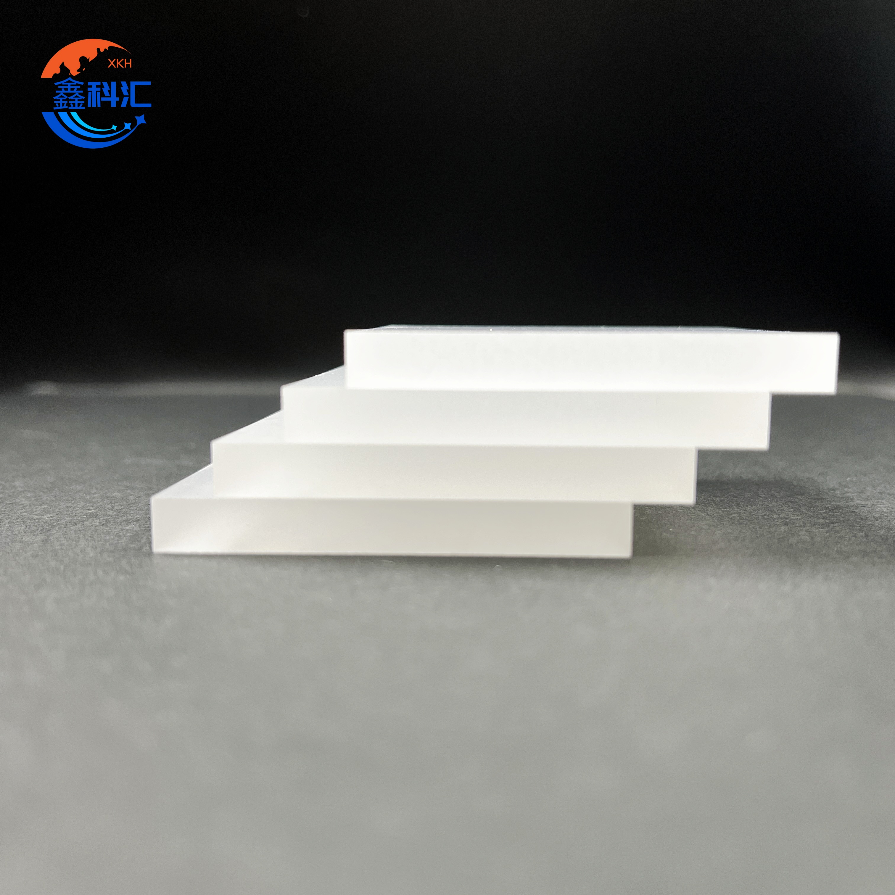
Sapphire Square Blank Substrate – Optical, Semiconductor, and Test Wafer


Detailed Diagram


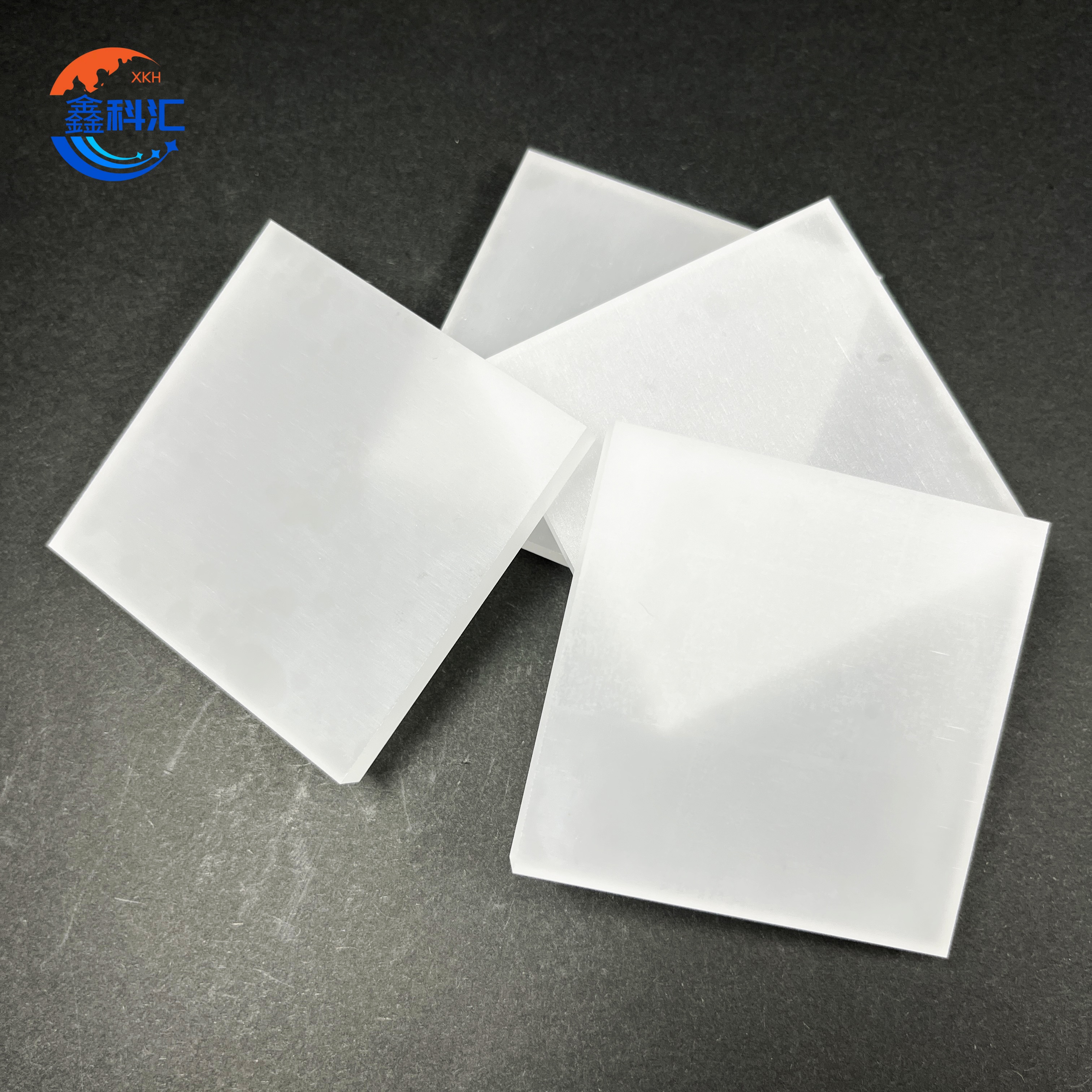
Overview of Sapphire Square Blank Substrate
The sapphire square blank substrate, as depicted in the image, is a high-purity single-crystal aluminum oxide (Al₂O₃) component designed for use in advanced optical engineering, semiconductor device manufacturing, and precision equipment testing. Renowned for its exceptional physical and chemical properties, sapphire has become one of the most indispensable materials in industries that demand extreme durability, stability, and optical performance. Produced through sophisticated crystal growth methods, such as the Kyropoulos (KY), Heat Exchange Method (HEM), or Czochralski (CZ) processes, these square blanks are meticulously manufactured to meet the highest quality standards.
Key Features of Sapphire Square Blank Substrate
Sapphire is a uniaxial, anisotropic crystal with a hexagonal lattice structure, offering an unparalleled combination of mechanical strength, thermal stability, and chemical resistance. With a Mohs hardness rating of 9, sapphire is second only to diamond in terms of scratch resistance, ensuring exceptional longevity even under abrasive industrial conditions. Its melting point exceeds 2000°C, allowing reliable performance in high-temperature environments, while its low dielectric loss makes it a preferred substrate material for RF and high-frequency electronic applications.
In the optical domain, sapphire exhibits a broad transmission range from deep ultraviolet (~200nm) through visible to mid-infrared (~5000nm), with excellent optical homogeneity and low birefringence when properly oriented. These properties make sapphire square blanks indispensable in optics-intensive fields such as laser systems, photonics, spectroscopy, and imaging.
Manufacturing and Processing
Each sapphire square blank substrate undergoes a stringent production process, beginning with high-purity raw alumina powders subjected to controlled crystal growth in high-temperature furnaces. After the bulk crystal is grown, it is precisely oriented (commonly C-plane (0001), A-plane (11-20), or R-plane (1-102)) to suit application-specific requirements. The crystal is then sliced into square blanks with diamond-coated saws, followed by precision lapping to achieve thickness uniformity. For optical and semiconductor applications, surfaces can be polished to atomic-level smoothness, meeting stringent flatness, parallelism, and surface roughness specifications.
Key Advantages
-
Outstanding Optical Transparency – Wideband transmission from UV to IR makes it ideal for optical windows, laser cavities, and sensor covers.
-
Superior Mechanical Strength – High compressive strength, fracture toughness, and scratch resistance ensure longevity in high-stress environments.
-
Thermal & Chemical Stability – Resistant to thermal shock, high temperatures, and aggressive chemicals, maintaining integrity during semiconductor processing and harsh environmental exposure.
-
Precise Dimensional Control – Achievable thickness tolerances within ±5µm and surface flatness up to λ/10 (at 632.8nm), critical for photolithography and wafer bonding applications.
-
Versatility – Suitable for a variety of applications including optical components, epitaxial growth substrates, and machine test wafers.
Applications
-
Optical Applications: Utilized as windows, filters, laser gain medium holders, protective covers for sensors, and photonics substrates due to its optical clarity and durability.
-
Semiconductor Substrates: Serves as a fundamental base for GaN-based LEDs, power electronics (SiC-on-sapphire structures), RF devices, and microelectronic circuits, where thermal conductivity and chemical resistance are paramount.
-
Equipment Test and Dummy Wafers: Frequently employed as test substrates in semiconductor fabrication lines, used for machine calibration, process simulation, and endurance testing of etching, deposition, or inspection equipment.
-
Scientific Research: Essential in experimental setups requiring inert, transparent, and mechanically stable platforms for optical, electrical, and materials studies.
FAQ
Q1: What is the advantage of using a square sapphire blank over a round wafer?
A: Square blanks provide maximum usable area for custom cutting, device fabrication, or machine testing, reducing material waste and cost.
Q2: Can sapphire substrates withstand semiconductor processing environments?
A: Yes, sapphire substrates maintain stability under high temperatures, plasma etching, and chemical treatments common in semiconductor fabrication.
Q3: Is surface orientation important for my application?
A: Absolutely. C-plane sapphire is widely used for GaN epitaxy in LED production, while A-plane and R-plane orientations are preferred for specific optical or piezoelectric applications.
Q4: Are these blanks available with custom coatings?
A: Yes, anti-reflective, dielectric, or conductive coatings can be applied to meet specific optical or electronic requirements.
About Us
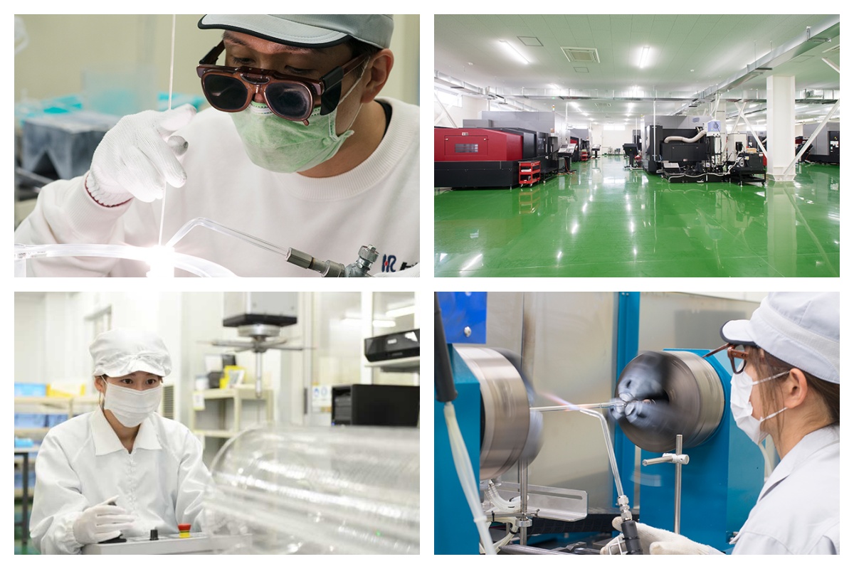
XKH specializes in high-tech development, production, and sales of special optical glass and new crystal materials. Our products serve optical electronics, consumer electronics, and the military. We offer Sapphire optical components, mobile phone lens covers, Ceramics, LT, Silicon Carbide SIC, Quartz, and semiconductor crystal wafers. With skilled expertise and cutting-edge equipment, we excel in non-standard product processing, aiming to be a leading optoelectronic materials high-tech enterprise.