Wafer Substrates as Key Materials in Semiconductor Devices
Wafer substrates are the physical carriers of semiconductor devices, and their material properties directly determine device performance, cost, and application fields. Below are the main types of wafer substrates along with their advantages and disadvantages:
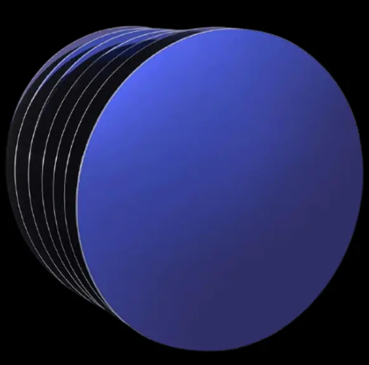
1. Silicon (Si)
-
Market Share: Accounts for more than 95% of the global semiconductor market.
-
Advantages:
-
Low cost: Abundant raw materials (silicon dioxide), mature manufacturing processes, and strong economies of scale.
-
High process compatibility: CMOS technology is highly mature, supporting advanced nodes (e.g., 3nm).
-
Excellent crystal quality: Large-diameter wafers (mainly 12-inch, 18-inch under development) with low defect density can be grown.
-
Stable mechanical properties: Easy to cut, polish, and handle.
-
-
Disadvantages:
-
Narrow bandgap (1.12 eV): High leakage current at elevated temperatures, limiting power device efficiency.
-
Indirect bandgap: Very low light emission efficiency, unsuitable for optoelectronic devices such as LEDs and lasers.
-
Limited electron mobility: Inferior high-frequency performance compared to compound semiconductors.
-
-
Applications: High-frequency RF devices (5G/6G), optoelectronic devices (lasers, solar cells).
-
Advantages:
-
High electron mobility (5–6× that of silicon): Suitable for high-speed, high-frequency applications such as millimeter-wave communication.
-
Direct bandgap (1.42 eV): High-efficiency photoelectric conversion, the foundation of infrared lasers and LEDs.
-
High temperature and radiation resistance: Suitable for aerospace and harsh environments.
-
-
Disadvantages:
-
High cost: Scarce material, difficult crystal growth (prone to dislocations), limited wafer size (mainly 6-inch).
-
Brittle mechanics: Prone to fracture, resulting in low processing yield.
-
Toxicity: Arsenic requires strict handling and environmental controls.
-
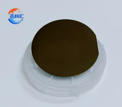
3. Silicon Carbide (SiC)
-
Applications: High-temperature and high-voltage power devices (EV inverters, charging stations), aerospace.
-
Advantages:
-
Wide bandgap (3.26 eV): High breakdown strength (10× that of silicon), high-temperature tolerance (operating temperature >200 °C).
-
High thermal conductivity (≈3× silicon): Excellent heat dissipation, enabling higher system power density.
-
Low switching loss: Improves power conversion efficiency.
-
-
Disadvantages:
-
Challenging substrate preparation: Slow crystal growth (>1 week), difficult defect control (micropipes, dislocations), extremely high cost (5–10× silicon).
-
Small wafer size: Mainly 4–6 inch; 8-inch still under development.
-
Difficult to process: Very hard (Mohs 9.5), making cutting and polishing time-consuming.
-
4. Gallium Nitride (GaN)
-
Applications: High-frequency power devices (fast charging, 5G base stations), blue LEDs/lasers.
-
Advantages:
-
Ultra-high electron mobility + wide bandgap (3.4 eV): Combines high-frequency (>100 GHz) and high-voltage performance.
-
Low on-resistance: Reduces device power loss.
-
Heteroepitaxy compatible: Commonly grown on silicon, sapphire, or SiC substrates, reducing cost.
-
-
Disadvantages:
-
Bulk single-crystal growth difficult: Heteroepitaxy is mainstream, but lattice mismatch introduces defects.
-
High cost: Native GaN substrates are very expensive (a 2-inch wafer can cost several thousand USD).
-
Reliability challenges: Phenomena such as current collapse require optimization.
-
5. Indium Phosphide (InP)
-
Applications: High-speed optical communications (lasers, photodetectors), terahertz devices.
-
Advantages:
-
Ultra-high electron mobility: Supports >100 GHz operation, outperforming GaAs.
-
Direct bandgap with wavelength matching: Core material for 1.3–1.55 μm optical fiber communications.
-
-
Disadvantages:
-
Brittle and very expensive: Substrate cost exceeds 100× silicon, limited wafer sizes (4–6 inch).
-
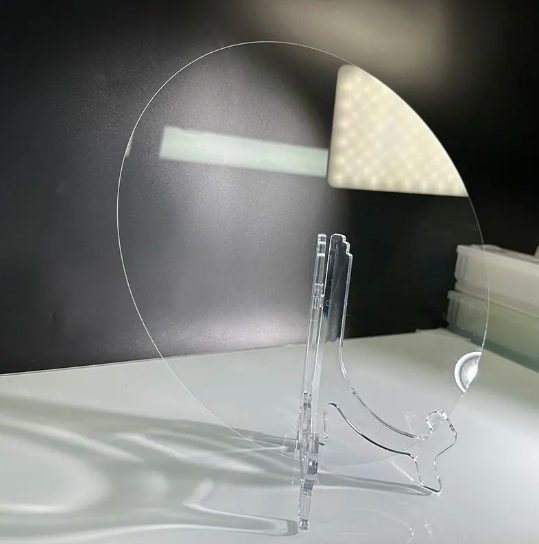
6. Sapphire (Al₂O₃)
-
Applications: LED lighting (GaN epitaxial substrate), consumer electronics cover glass.
-
Advantages:
-
Low cost: Much cheaper than SiC/GaN substrates.
-
Excellent chemical stability: Corrosion-resistant, highly insulating.
-
Transparency: Suitable for vertical LED structures.
-
-
Disadvantages:
-
Large lattice mismatch with GaN (>13%): Causes high defect density, requiring buffer layers.
-
Poor thermal conductivity (~1/20 of silicon): Limits performance of high-power LEDs.
-
7. Ceramic Substrates (AlN, BeO, etc.)
-
Applications: Heat spreaders for high-power modules.
-
Advantages:
-
Insulating + high thermal conductivity (AlN: 170–230 W/m·K): Suitable for high-density packaging.
-
-
Disadvantages:
-
Non-single-crystal: Cannot directly support device growth, used only as packaging substrates.
-
8. Special Substrates
-
SOI (Silicon on Insulator):
-
Structure: Silicon/SiO₂/silicon sandwich.
-
Advantages: Reduces parasitic capacitance, radiation-hardened, leakage suppression (used in RF, MEMS).
-
Disadvantages: 30–50% more expensive than bulk silicon.
-
-
Quartz (SiO₂): Used in photomasks and MEMS; high-temperature resistance but very brittle.
-
Diamond: Highest thermal conductivity substrate (>2000 W/m·K), under R&D for extreme heat dissipation.
Comparative Summary Table
| Substrate | Bandgap (eV) | Electron Mobility (cm²/V·s) | Thermal Conductivity (W/m·K) | Main Wafer Size | Core Applications | Cost |
|---|---|---|---|---|---|---|
| Si | 1.12 | ~1,500 | ~150 | 12-inch | Logic / Memory Chips | Lowest |
| GaAs | 1.42 | ~8,500 | ~55 | 4–6 inch | RF / Optoelectronics | High |
| SiC | 3.26 | ~900 | ~490 | 6-inch (8-inch R&D) | Power devices / EV | Very High |
| GaN | 3.4 | ~2,000 | ~130–170 | 4–6 inch (heteroepitaxy) | Fast charging / RF / LEDs | High (heteroepitaxy: medium) |
| InP | 1.35 | ~5,400 | ~70 | 4–6 inch | Optical communications / THz | Extremely High |
| Sapphire | 9.9 (insulator) | – | ~40 | 4–8 inch | LED substrates | Low |
Key Factors for Substrate Selection
-
Performance requirements: GaAs/InP for high-frequency; SiC for high-voltage, high-temperature; GaAs/InP/GaN for optoelectronics.
-
Cost constraints: Consumer electronics favor silicon; high-end fields can justify SiC/GaN premiums.
-
Integration complexity: Silicon remains irreplaceable for CMOS compatibility.
-
Thermal management: High-power applications prefer SiC or diamond-based GaN.
-
Supply chain maturity: Si > Sapphire > GaAs > SiC > GaN > InP.
Future Trend
Heterogeneous integration (e.g., GaN-on-Si, GaN-on-SiC) will balance performance and cost, driving advancements in 5G, electric vehicles, and quantum computing.
Post time: Aug-21-2025