Introduction to silicon carbide
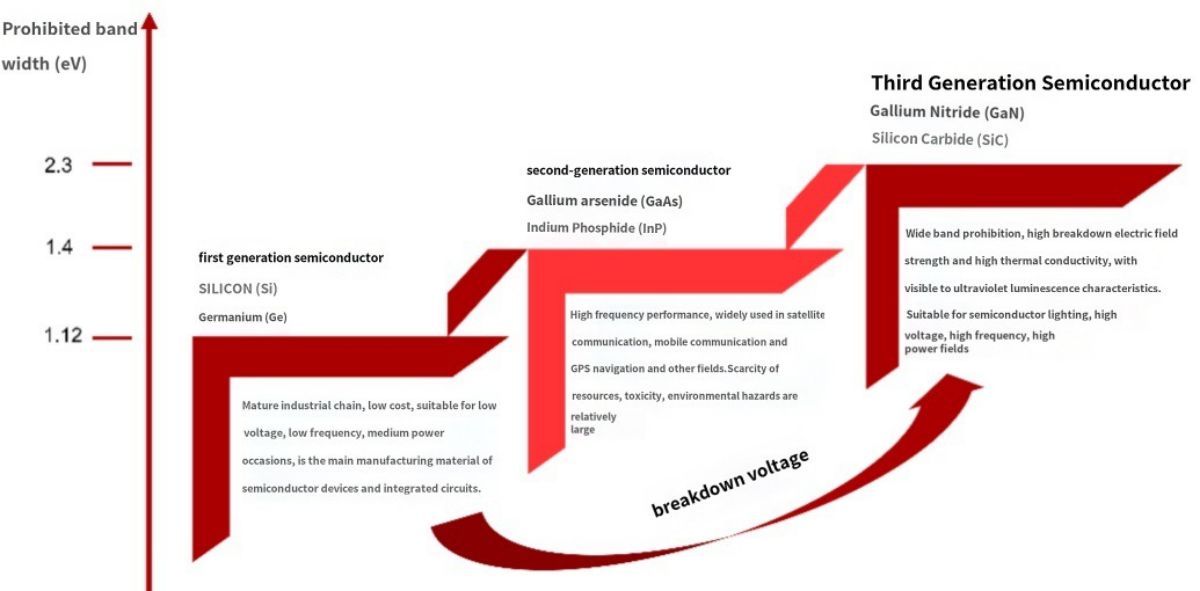
Silicon carbide (SiC) is a compound semiconductor material composed of carbon and silicon, which is one of the ideal materials for making high temperature, high frequency, high power and high voltage devices. Compared with the traditional silicon material (Si), the band gap of silicon carbide is 3 times that of silicon. The thermal conductivity is 4-5 times that of silicon; The breakdown voltage is 8-10 times that of silicon; The electronic saturation drift rate is 2-3 times that of silicon, which meets the needs of modern industry for high power, high voltage and high frequency. It is mainly used for the production of high-speed, high-frequency, high-power and light-emitting electronic components. The downstream application fields include smart grid, new energy vehicles, photovoltaic wind power, 5G communication, etc. Silicon carbide diodes and MOSFETs have been commercially applied.
High temperature resistance. The band gap width of silicon carbide is 2-3 times that of silicon, the electrons are not easy to transition at high temperatures, and can withstand higher operating temperatures, and the thermal conductivity of silicon carbide is 4-5 times that of silicon, making the device heat dissipation easier and the limit operating temperature higher. The high temperature resistance can significantly increase power density while reducing the requirements on the cooling system, making the terminal lighter and smaller.
Withstand high pressure. The breakdown electric field strength of silicon carbide is 10 times that of silicon, which can withstand higher voltages and is more suitable for high-voltage devices.
High frequency resistance. Silicon carbide has a saturated electron drift rate twice that of silicon, resulting in the absence of current tailing during the shutdown process, which can effectively improve the switching frequency of the device and realize the miniaturization of the device.
Low energy loss. Compared with silicon material, silicon carbide has very low on-resistance and low on-loss. At the same time, the high band-gap width of silicon carbide greatly reduces the leakage current and the power loss. In addition, the silicon carbide device does not have current trailing phenomenon during the shutdown process, and the switching loss is low.
Silicon carbide industry chain
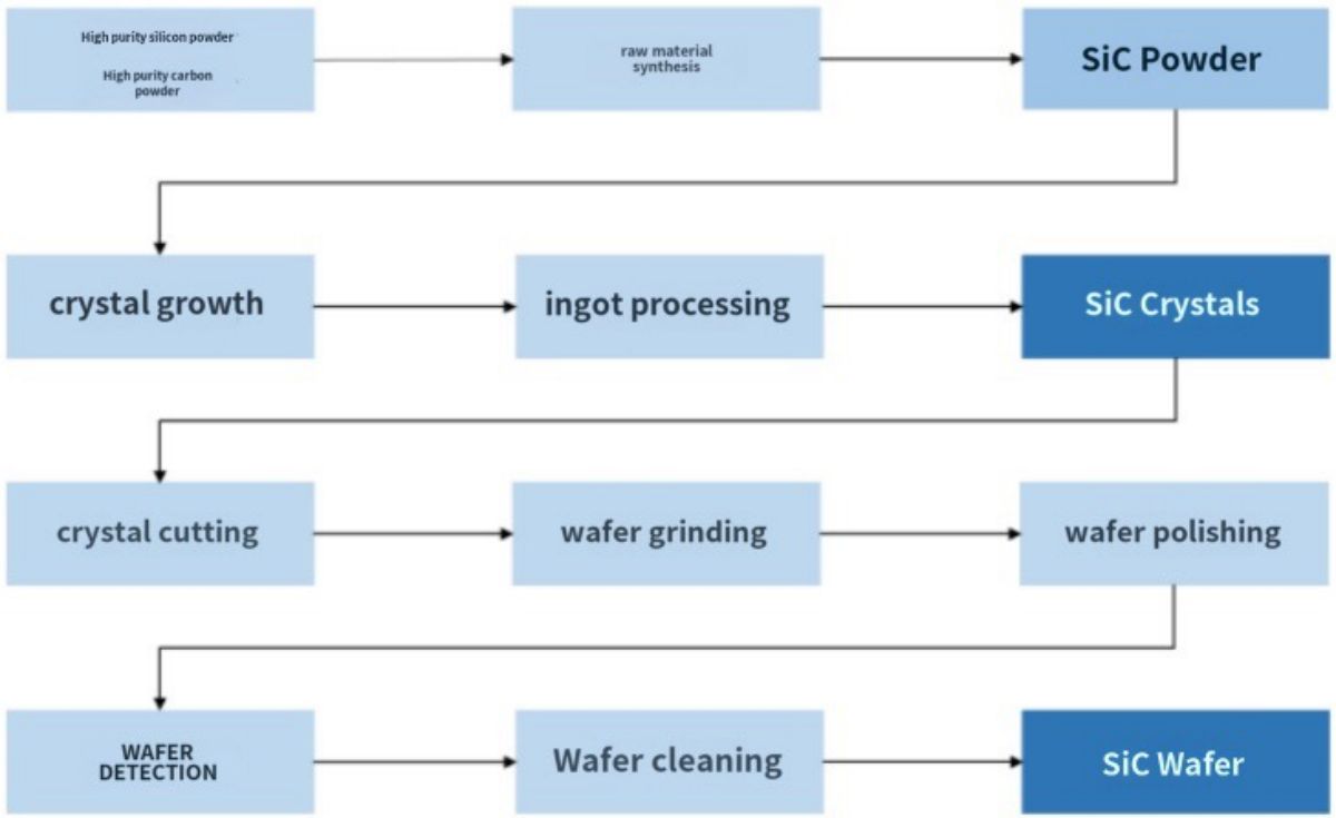
It mainly includes substrate, epitaxy, device design, manufacturing, sealing and so on. Silicon carbide from the material to the semiconductor power device will experience single crystal growth, ingot slicing, epitaxial growth, wafer design, manufacturing, packaging and other processes. After the synthesis of silicon carbide powder, the silicon carbide ingot is made first, and then the silicon carbide substrate is obtained by slicing, grinding and polishing, and the epitaxial sheet is obtained by epitaxial growth. The epitaxial wafer is made of silicon carbide through lithography, etching, ion implantation, metal passivation and other processes, the wafer is cut into die, the device is packaged, and the device is combined into a special shell and assembled into a module.
Upstream of the industry chain 1: substrate - crystal growth is the core process link
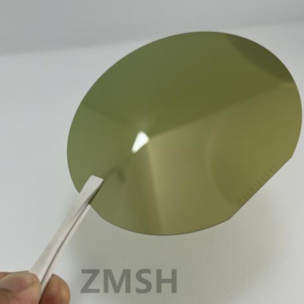
Silicon carbide substrate accounts for about 47% of the cost of silicon carbide devices, the highest manufacturing technical barriers, the largest value, is the core of the future large-scale industrialization of SiC.
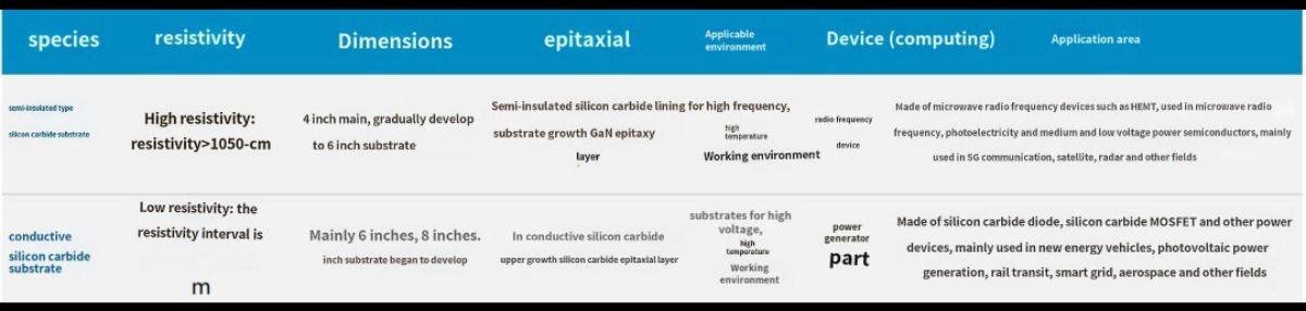
From the perspective of electrochemical property differences, silicon carbide substrate materials can be divided into conductive substrates (resistivity region 15~30mΩ·cm) and semi-insulated substrates (resistivity higher than 105Ω·cm). These two kinds of substrates are used to manufacture discrete devices such as power devices and radio frequency devices respectively after epitaxial growth. Among them, semi-insulated silicon carbide substrate is mainly used in the manufacture of gallium nitride RF devices, photoelectric devices and so on. By growing gan epitaxial layer on semi-insulated SIC substrate, the sic epitaxial plate is prepared, which can be further prepared into HEMT gan iso-nitride RF devices. Conductive silicon carbide substrate is mainly used in the manufacture of power devices. Different from the traditional silicon power device manufacturing process, the silicon carbide power device can not be directly made on the silicon carbide substrate, the silicon carbide epitaxial layer needs to be grown on the conductive substrate to obtain the silicon carbide epitaxial sheet, and the epitaxial layer is manufactured on the Schottky diode, MOSFET, IGBT and other power devices.
Silicon carbide powder was synthesized from high purity carbon powder and high purity silicon powder, and different sizes of silicon carbide ingot were grown under special temperature field, and then silicon carbide substrate was produced through multiple processing processes. The core process includes:
Raw material synthesis: The high-purity silicon powder + toner is mixed according to the formula, and the reaction is carried out in the reaction chamber under the high temperature condition above 2000°C to synthesize the silicon carbide particles with specific crystal type and particle size. Then through the crushing, screening, cleaning and other processes, to meet the requirements of high purity silicon carbide powder raw materials.
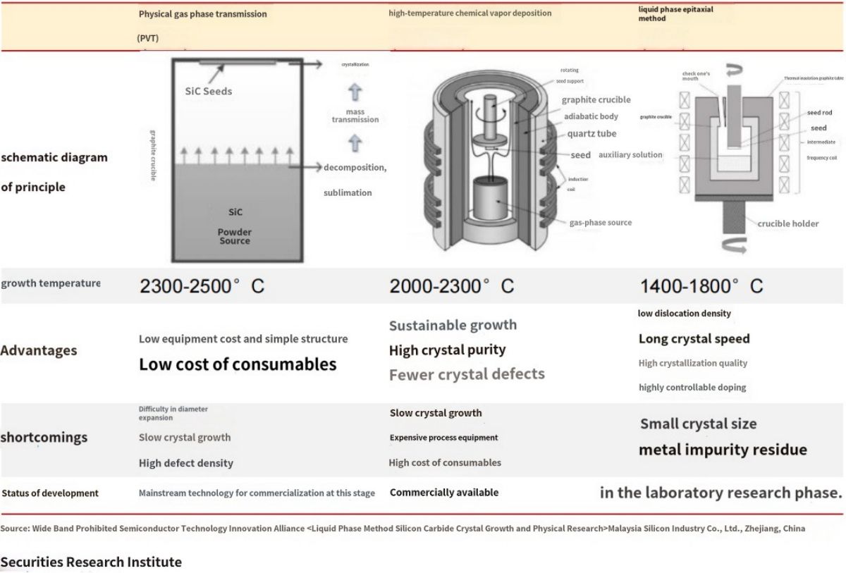
Crystal growth is the core process of silicon carbide substrate manufacturing, which determines the electrical properties of silicon carbide substrate. At present, the main methods for crystal growth are physical vapor transfer (PVT), high temperature chemical vapor deposition (HT-CVD) and liquid phase epitaxy (LPE). Among them, PVT method is the mainstream method for commercial growth of SiC substrate at present, with the highest technical maturity and the most widely used in engineering.
The preparation of SiC substrate is difficult, leading to its high price
Temperature field control is difficult: Si crystal rod growth only needs 1500℃, while SiC crystal rod needs to be grown at a high temperature above 2000℃, and there are more than 250 SiC isomers, but the main 4H-SiC single crystal structure for the production of power devices, if not precise control, will get other crystal structures. In addition, the temperature gradient in the crucible determines the rate of SiC sublimation transfer and the arrangement and growth mode of gaseous atoms on the crystal interface, which affects the crystal growth rate and crystal quality, so it is necessary to form a systematic temperature field control technology. Compared with Si materials, the difference in SiC production is also in high temperature processes such as high temperature ion implantation, high temperature oxidation, high temperature activation, and the hard mask process required by these high temperature processes.
Slow crystal growth: the growth rate of Si crystal rod can reach 30 ~ 150mm/h, and the production of 1-3m silicon crystal rod only takes about 1 day; SiC crystal rod with PVT method as an example, the growth rate is about 0.2-0.4mm/h, 7 days to grow less than 3-6cm, the growth rate is less than 1% of the silicon material, the production capacity is extremely limited.
High product parameters and low yield: the core parameters of SiC substrate include microtubule density, dislocation density, resistivity, warpage, surface roughness, etc. It is a complex system engineering to arrange atoms in a closed high-temperature chamber and complete crystal growth, while controlling parameter indexes.
The material has high hardness, high brittleness, long cutting time and high wear: SiC Mohs hardness of 9.25 is second only to diamond, which leads to a significant increase in the difficulty of cutting, grinding and polishing, and it takes approximately 120 hours to cut 35-40 pieces of a 3cm thick ingot. In addition, due to the high brittleness of SiC, wafer processing wear will be more, and the output ratio is only about 60%.
Development trend: Size increase + price decrease
The global SiC market 6-inch volume production line is maturing, and leading companies have entered the 8-inch market. Domestic development projects are mainly 6 inches. At present, although most domestic companies are still based on 4-inch production lines, but the industry is gradually expanding to 6-inch, with the maturity of 6-inch supporting equipment technology, domestic SiC substrate technology is also gradually improving the economies of scale of large-size production lines will be reflected, and the current domestic 6-inch mass production time gap has narrowed to 7 years. The larger wafer size can bring about an increase in the number of single chips, improve the yield rate, and reduce the proportion of edge chips, and the cost of research and development and yield loss will be maintained at about 7%, thereby improving wafer utilization.
There are still many difficulties in device design
The commercialization of SiC diode is gradually improved, at present, a number of domestic manufacturers have designed SiC SBD products, medium and high voltage SiC SBD products have good stability, in the vehicle OBC, the use of SiC SBD+SI IGBT to achieve stable current density. At present, there are no barriers in the patent design of SiC SBD products in China, and the gap with foreign countries is small.
SiC MOS still has many difficulties, there is still a gap between SiC MOS and overseas manufacturers, and the relevant manufacturing platform is still under construction. At present, ST, Infineon, Rohm and other 600-1700V SiC MOS have achieved mass production and signed and shipped with many manufacturing industries, while the current domestic SiC MOS design has been basically completed, a number of design manufacturers are working with fabs at the wafer flow stage, and later customer verification still needs some time, so there is still a long time from large-scale commercialization.
At present, the planar structure is the mainstream choice, and the trench type is widely used in the high-pressure field in the future. Planar structure SiC MOS manufacturers are many, the planar structure is not easy to produce local breakdown problems compared with the groove, affecting the stability of the work, in the market below 1200V has a wide range of application value, and the planar structure is relatively simple in the manufacturing end, to meet the manufacturability and cost control two aspects. The groove device has the advantages of extremely low parasitic inductance, fast switching speed, low loss and relatively high performance.
2--SiC wafer news
Silicon carbide market production and sales growth, pay attention to structural imbalance between supply and demand
With the rapid growth of the market demand for high-frequency and high-power power electronics, the physical limit bottleneck of silicon-based semiconductor devices has gradually become prominent, and the third-generation semiconductor materials represented by silicon carbide (SiC) have gradually become industrialized. From the material performance point of view, silicon carbide has 3 times the band gap width of silicon material, 10 times the critical breakdown electric field strength, 3 times the thermal conductivity, so silicon carbide power devices are suitable for high frequency, high pressure, high temperature and other applications, help to improve the efficiency and power density of power electronic systems.
At present, SiC diodes and SiC MOSFETs have gradually moved to the market, and there are more mature products, among which SiC diodes are widely used instead of silicon-based diodes in some fields because they do not have the advantage of reverse recovery charge; SiC MOSFET is also gradually used in automotive, energy storage, charging pile, photovoltaic and other fields; In the field of automotive applications, the trend of modularization is becoming more and more prominent, the superior performance of SiC needs to rely on advanced packaging processes to achieve, technically with relatively mature shell sealing as the mainstream, the future or to plastic sealing development, its customized development characteristics are more suitable for SiC modules.
Silicon carbide price decline speed or beyond imagination
The application of silicon carbide devices is mainly limited by the high cost, the price of SiC MOSFET under the same level is 4 times higher than that of Si based IGBT, this is because the process of silicon carbide is complex, in which the growth of single crystal and epitaxial is not only harsh on the environment, but also the growth rate is slow, and the single crystal processing into the substrate must go through the cutting and polishing process. Based on its own material characteristics and immature processing technology, the yield of domestic substrate is less than 50%, and various factors lead to high substrate and epitaxial prices.
However, the cost composition of silicon carbide devices and silicon-based devices is diametrically opposite, the substrate and epitaxial costs of the front channel account for 47% and 23% of the entire device respectively, totalling about 70%, the device design, manufacturing and sealing links of the back channel account for only 30%, the production cost of silicon-based devices is mainly concentrated in the wafer manufacturing of the back channel about 50%, and the substrate cost accounts for only 7%. The phenomenon of the value of silicon carbide industry chain upside down means that upstream substrate epitaxy manufacturers have the core right to speak, which is the key to the layout of domestic and foreign enterprises.
From the dynamic point of view on the market, reducing the cost of silicon carbide, in addition to improving the silicon carbide long crystal and slicing process, is to expand the wafer size, which is also the mature path of semiconductor development in the past, Wolfspeed data show that the silicon carbide substrate upgrade from 6 inches to 8 inches, qualified chip production can increase by 80%-90%, and help improve the yield. Can reduce the combined unit cost by 50%.
2023 is known as the "8-inch SiC first year", this year, domestic and foreign silicon carbide manufacturers are accelerating the layout of 8-inch silicon carbide, such as Wolfspeed crazy investment of 14.55 billion US dollars for silicon carbide production expansion, an important part of which is the construction of 8-inch SiC substrate manufacturing plant, To ensure the future supply of 200 mm SiC bare metal to a number of companies; Domestic Tianyue Advanced and Tianke Heda have also signed long-term agreements with Infineon to supply 8-inch silicon carbide substrates in the future.
Starting from this year, silicon carbide will accelerate from 6 inches to 8 inches, Wolfspeed expects that by 2024, the unit chip cost of 8 inches substrate compared to the unit chip cost of 6 inches substrate in 2022 will be reduced by more than 60%, and the cost decline will further open the application market, Ji Bond Consulting research data pointed out. The current market share of 8-inch products is less than 2%, and the market share is expected to grow to about 15% by 2026.
In fact, the rate of decline in the price of silicon carbide substrate may exceed many people's imagination, the current market offer of 6-inch substrate is 4000-5000 yuan/piece, compared with the beginning of the year has fallen a lot, is expected to fall below 4000 yuan next year, it is worth noting that some manufacturers in order to get the first market, has reduced the sales price to the cost line below, Opened the model of the price war, mainly concentrated in the silicon carbide substrate supply has been relatively sufficient in the low-voltage field, domestic and foreign manufacturers are aggressively expanding production capacity, or let the silicon carbide substrate oversupply stage earlier than imagined.
Post time: Jan-19-2024