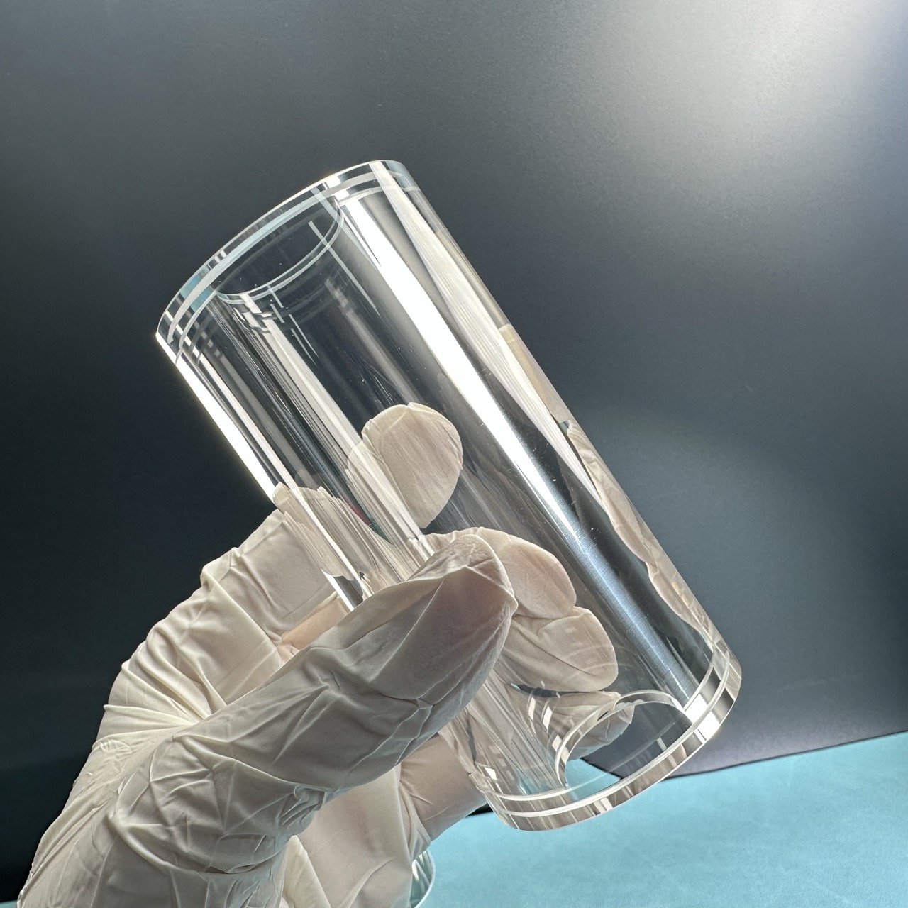
LiNbO₃ Wafers 2inch-8inch Thickness 0.1 ~ 0.5mm TTV 3µm Custom


Technical parameters
| Material | Optical Grade LiNbO3 wafes | |
| Curie Temp | 1142±2.0℃ | |
| Cutting Angle | X/Y/Z etc | |
| Diameter/size | 2"/3"/4"/6"/8" | |
| Tol(±) | <0.20 mm | |
| Thickness | 0.1 ~ 0.5mm or more | |
| Primary Flat | 16mm/22mm /32mm | |
| TTV | <3µm | |
| Bow | -30<bow<30 | |
| Warp | <40µm | |
| Orientation Flat | All available | |
| Surface Type | Single Side Polished /Double Sides Polished | |
| Polished side Ra | <0.5nm | |
| S/D | 20/10 | |
| Edge Criteria | R=0.2mm or Bullnose | |
| Optical doped | Fe/Zn/MgO etc for optical grade LN< wafers | |
| Wafer Surface Criteria | Refractive index | No=2.2878/Ne=2.2033 @632nm wavelength |
| Contamination, | None | |
| Particles ¢>0.3 µ m | <= 30 | |
| Scratch , Chipping | None | |
| Defect | No edge cracks, scratches, saw marks, stains | |
| Packaging | Qty/Wafer box | 25pcs per box |
Core Attributes of Our LiNbO₃ Wafers
1.Photonic Performance Characteristics
Our LiNbO₃ Wafers exhibit extraordinary light-matter interaction capabilities, with nonlinear optical coefficients reaching 42 pm/V - enabling efficient wavelength conversion processes critical for quantum photonics. The substrates maintain >72% transmission across 320-5200nm, with specially engineered versions achieving <0.2dB/cm propagation loss at telecom wavelengths.
2.Acoustic Wave Engineering
The crystalline structure of our LiNbO₃ Wafers supports surface wave velocities exceeding 3800 m/s, permitting resonator operation up to 12GHz. Our proprietary polishing techniques yield surface acoustic wave (SAW) devices with insertion losses under 1.2dB, while maintaining temperature stability within ±15ppm/°C.
3.Environmental Resilience
Engineered to withstand extreme conditions, our LiNbO₃ Wafers maintain functionality from cryogenic temperatures to 500°C operational environments. The material demonstrates exceptional radiation hardness, withstanding >1Mrad total ionizing dose without significant performance degradation.
4.Application-Specific Configurations
We offer domain-engineered variants including:
Periodically poled structures with 5-50μm domain periods
Ion-sliced thin films for hybrid integration
Metamaterial-enhanced versions for specialized applications
Implementation Scenarios for LiNbO₃ Wafers
1.Next-Gen Optical Networks
LiNbO₃ Wafers serve as the backbone for terabit-scale optical transceivers, enabling 800Gbps coherent transmission through advanced nested modulator designs. Our substrates are increasingly adopted for co-packaged optics implementations in AI/ML accelerator systems.
2.6G RF Frontends
The latest generation of LiNbO₃ Wafers supports ultra-wideband filtering up to 20GHz, addressing the spectrum needs of emerging 6G standards. Our materials enable novel acoustic resonator architectures with Q factors surpassing 2000.
3.Quantum Information Systems
Precision-poled LiNbO₃ Wafers form the foundation for entangled photon sources with >90% pair generation efficiency. Our substrates are enabling breakthroughs in photonic quantum computing and secure communication networks.
4.Advanced Sensing Solutions
From automotive LiDAR operating at 1550nm to ultra-sensitive gravimetric sensors, LiNbO₃ Wafers provide the critical transduction platform. Our materials enable sensor resolutions down to single-molecule detection levels.
Key Advantages of LiNbO₃Wafers
1. Unparalleled Electro-Optic Performance
Exceptionally High Electro-Optic Coefficient (r₃₃~30-32 pm/V): Represents the industry benchmark for commercial lithium niobate wafers, enabling 200Gbps+ high-speed optical modulators that far surpass the performance limits of silicon-based or polymer solutions.
Ultra-Low Insertion Loss (<0.1 dB/cm): Achieved through nanoscale polishing (Ra<0.3 nm) and anti-reflection (AR) coatings, significantly enhancing the energy efficiency of optical communication modules.
2. Superior Piezoelectric & Acoustic Properties
Ideal for High-Frequency SAW/BAW Devices: With acoustic velocities of 3500-3800 m/s, these wafers support 6G mmWave (24-100 GHz) filter designs featuring insertion losses <1.0 dB.
High Electromechanical Coupling Coefficient (K²~0.25%): Enhances bandwidth and signal selectivity in RF front-end components, making them suitable for 5G/6G base stations and satellite communications.
3. Broadband Transparency & Nonlinear Optical Effects
Ultra-Wide Optical Transmission Window (350-5000 nm): Covers UV to mid-IR spectra, enabling applications such as:
Quantum Optics: Periodically poled (PPLN) configurations achieve >90% efficiency in entangled photon pair generation.
Laser Systems: Optical parametric oscillation (OPO) delivers tunable wavelength output (1-10 μm).
Exceptional Laser Damage Threshold (>1 GW/cm²): Meets stringent requirements for high-power laser applications.
4. Extreme Environmental Stability
High-Temperature Resistance (Curie point: 1140°C): Maintains stable performance across -200°C to +500°C, ideal for:
Automotive Electronics (engine compartment sensors)
Spacecraft (deep-space optical components)
Radiation Hardness (>1 Mrad TID): Compliant with MIL-STD-883 standards, suitable for nuclear and defense electronics.
5. Customization & Integration Flexibility
Crystal Orientation & Doping Optimization:
X/Y/Z-cut wafers (±0.3° precision)
MgO doping (5 mol%) for enhanced optical damage resistance
Heterogeneous Integration Support:
Compatible with thin-film LiNbO₃-on-Insulator (LNOI) for hybrid integration with silicon photonics (SiPh)
Enables wafer-level bonding for co-packaged optics (CPO)
6. Scalable Production & Cost Efficiency
6-inch (150mm) Wafer Mass Production: Reduces unit costs by 30% compared to traditional 4-inch processes.
Rapid Delivery: Standard products ship in 3 weeks; small-batch prototypes (minimum 5 wafers) deliver in 10 days.
XKH Services
1. Material Innovation Lab
Our crystal growth experts collaborate with clients to develop application-specific LiNbO₃ Wafers formulations, including:
Low optical loss variants (<0.05dB/cm)
High-power handling configurations
Radiation-tolerant compositions
2. Rapid Prototyping Pipeline
From design to delivery in 10 business days for:
Custom orientation wafers
Patterned electrodes
Pre-characterized samples
3. Performance Certification
Every LiNbO₃ Wafer shipment includes:
Full spectroscopic characterization
Crystallographic orientation verification
Surface quality certification
4. Supply Chain Assurance
Dedicated production lines for critical applications
Buffer inventory for emergency orders
ITAR-compliant logistics network


Related Products
-

TVG process on quartz sapphire BF33 wafer Glass...
-
Sapphire Rods Industrial Applications sapphire ...
-

Sapphire ingot dia 4inch× 80mm Monocrystalline ...
-

Gallium Nitride (GaN) Epitaxial Grown on Sapphi...
-
Sapphire green for gemstone olive green artific...
-

Quartz crystal boat custom equipment for high t...