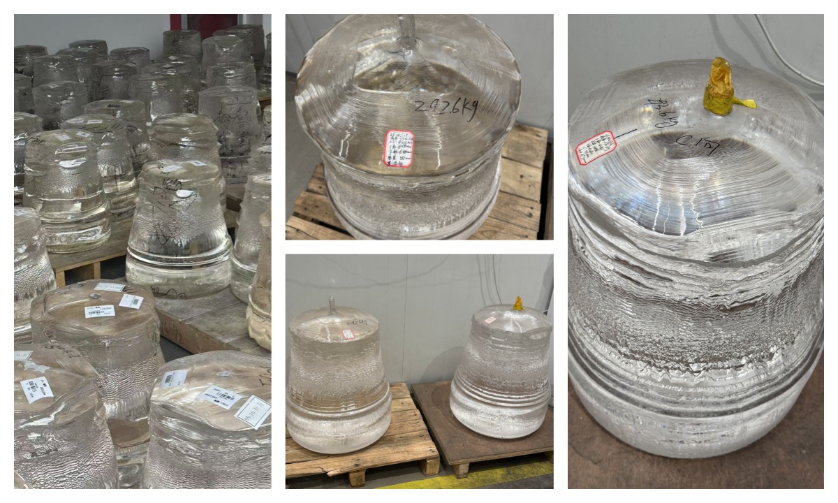
As-grown sapphire boule ingot crystal ky method


Detailed Diagram


Overview
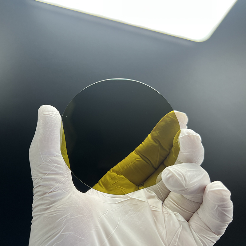
A sapphire boule is a large, as-grown single crystal of aluminum oxide (Al₂O₃) that serves as the upstream feedstock for sapphire wafers, optical windows, wear-resistant parts, and gem cutting. With Mohs 9 hardness, excellent thermal stability (melting point ~2050 °C), and broadband transparency from UV to mid-IR, sapphire is the benchmark material where durability, cleanliness, and optical quality must coexist.
We supply colorless and doped sapphire boules produced by industry-proven growth methods, optimized for GaN/AlGaN epitaxy, precision optics, and high-reliability industrial components.
Why Sapphire Boule from Us
-
Crystal quality first: low internal stress, low bubble/striae content, tight orientation control for downstream slicing and epitaxy.
-
Process flexibility: KY/HEM/CZ/Verneuil growth options to balance size, stress, and cost for your application.
-
Scalable geometry: cylindrical, carrot-shape, or block boules with custom flats, seed/end treatments, and reference planes.
-
Traceable & repeatable: batch records, metrology reports, and acceptance criteria aligned to your spec.
Growth Technologies
-
KY (Kyropoulos): Large-diameter, low-stress boules; favored for epi-grade wafers and optics where birefringence uniformity matters.
-
HEM (Heat-Exchanger Method): Excellent thermal gradients and stress control; attractive for thick optics and premium epi feedstock.
-
CZ (Czochralski): Strong control of orientation and reproducibility; good choice for consistent, high-yield slicing.
-
Verneuil (Flame-Fusion): Cost-efficient, high throughput; suitable for general optics, mechanical parts, and gem preforms.
Crystal Orientation, Geometry & Size
-
Standard orientations: c-plane (0001), a-plane (11-20), r-plane (1-102), m-plane (10-10); custom planes available.
-
Orientation accuracy: ≤ ±0.1° by Laue/XRD (tighter upon request).
-
Shapes: cylindrical or carrot-type boules, square/rectangular blocks, and rods.
-
Typical size envelope: Ø30–220 mm, length 50–400 mm (larger/smaller made to order).
-
End/Reference features: seed/end face machining, reference flats/notches, and fiducials for downstream alignment.
Material & Optical Properties
-
Composition: Single-crystal Al₂O₃, raw material purity ≥ 99.99%.
-
Density: ~3.98 g/cm³
-
Hardness: Mohs 9
-
Refractive index (589 nm): nₒ ≈ 1.768, nₑ ≈ 1.760 (negative uniaxial; Δn ≈ 0.008)
-
Transmission window: UV to ~5 µm (thickness- and impurity-dependent)
-
Thermal conductivity (300 K): ~25 W·m⁻¹·K⁻¹
-
CTE (20–300 °C): ~5–8 × 10⁻⁶ /K (orientation-dependent)
-
Young’s modulus: ~345 GPa
-
Electrical: Highly insulating (volume resistivity typically ≥ 10¹⁴ Ω·cm)
Grades & Options
-
Epitaxy Grade: Ultra-low bubbles/striae and minimized stress birefringence for high-yield GaN/AlGaN MOCVD wafers (2–8 inch and above downstream).
-
Optical Grade: High internal transmission and homogeneity for windows, lenses, and IR viewports.
-
General/Mechanical Grade: Durable, cost-optimized feedstock for watch crystals, buttons, wear parts, and housings.
-
Doping/Color:
-
Colorless (standard)
Cr:Al₂O₃ (ruby), Ti:Al₂O₃ (Ti:sapphire) preforms
Other chromophores (Fe/Ti) on request
-
Applications
Semiconductor: Substrates for GaN LEDs, micro-LEDs, power HEMTs, RF devices (sapphire wafer feedstock).
Optics & Photonics: High-temperature/pressure windows, IR viewports, laser cavity windows, detector covers.
Consumer & Wearables: Watch crystals, camera lens covers, fingerprint sensor covers, premium exterior parts.
Industrial & Aerospace: Nozzles, valve seats, seal rings, protective windows, and observation ports.
Laser/Crystal Growth: Ti:sapphire and ruby hosts from doped boules.
At-a-Glance Data (Typical, for reference)
| Parameter | Value (Typical) |
|---|---|
| Composition | Single-crystal Al₂O₃ (≥ 99.99% purity) |
| Orientation | c / a / r / m (custom on request) |
| Index @ 589 nm | nₒ ≈ 1.768, nₑ ≈ 1.760 |
| Transmission Range | ~0.2–5 µm (thickness-dependent) |
| Thermal Conductivity | ~25 W·m⁻¹·K⁻¹ (300 K) |
| CTE (20–300 °C) | ~5–8 × 10⁻⁶/K |
| Young’s Modulus | ~345 GPa |
| Density | ~3.98 g/cm³ |
| Hardness | Mohs 9 |
| Electrical | Insulating; volume resistivity ≥ 10¹⁴ Ω·cm |
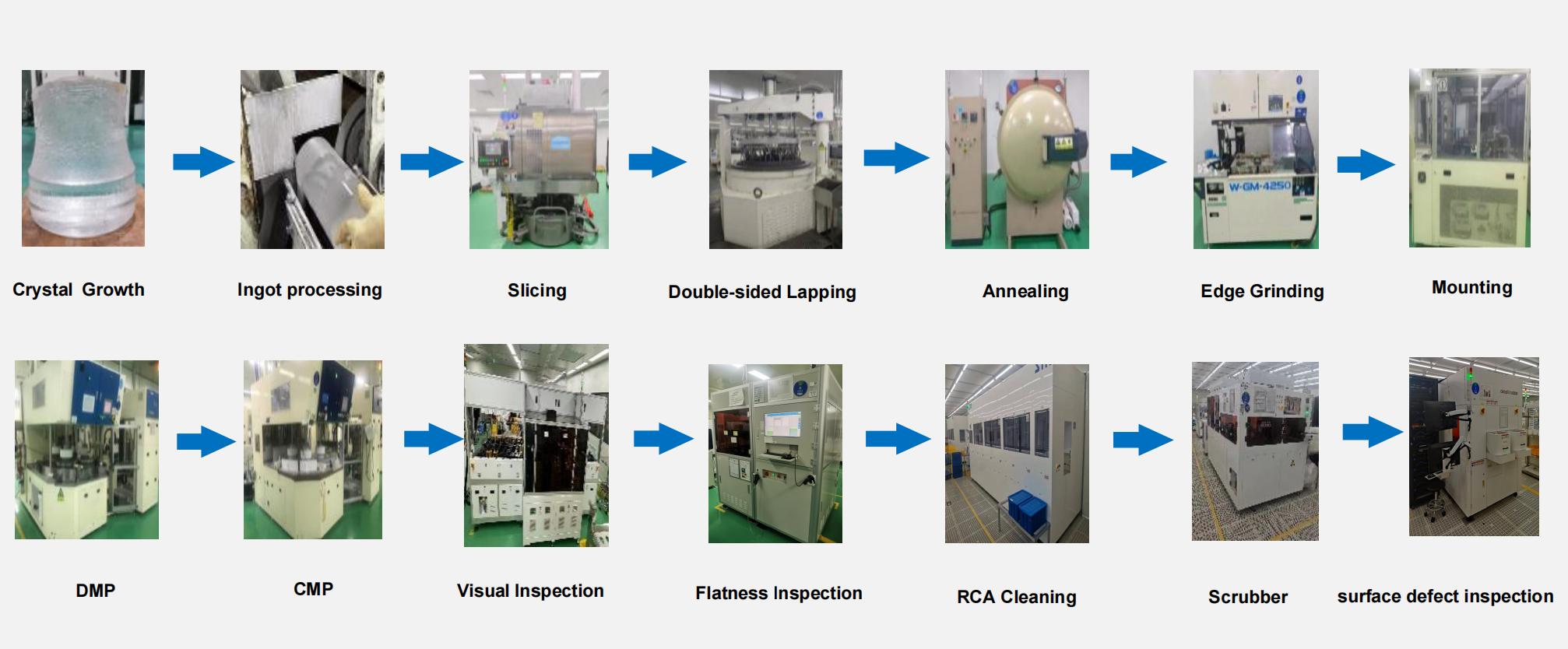
Sapphire Wafer Manufacturing Process
-
Crystal Growth
High-purity alumina (Al₂O₃) is melted and grown into a single sapphire crystal ingot using the Kyropoulos (KY) or Czochralski (CZ) method. -
Ingot Processing
The ingot is machined to a standard shape — trimming, diameter shaping, and end-face processing. -
Slicing
The sapphire ingot is sliced into thin wafers using a diamond wire saw. -
Double-sided Lapping
Both sides of the wafer are lapped to remove saw marks and achieve uniform thickness. -
Annealing
The wafers are heat-treated to release internal stress and improve crystal quality and transparency. -
Edge Grinding
The wafer edges are beveled to prevent chipping and cracking during further processing. -
Mounting
Wafers are mounted onto carriers or holders for precision polishing and inspection. -
DMP (Double-sided Mechanical Polishing)
The wafer surfaces are mechanically polished to improve surface smoothness. -
CMP (Chemical Mechanical Polishing)
A fine polishing step combining chemical and mechanical actions to create a mirror-like surface. -
Visual Inspection
Operators or automated systems check for visible surface defects. -
Flatness Inspection
Flatness and thickness uniformity are measured to ensure dimensional precision. -
RCA Cleaning
Standard chemical cleaning removes organic, metallic, and particulate contaminants. -
Scrubber Cleaning
Mechanical scrubbing removes remaining microscopic particles. -
Surface Defect Inspection
Automated optical inspection detects micro-defects such as scratches, pits, or contamination.
Sapphire Boule (Single-Crystal Al₂O₃) — FAQ
Q1: What is a sapphire boule?
A: An as-grown single crystal of aluminum oxide (Al₂O₃). It is the upstream “ingot” used to make sapphire wafers, optical windows, and high-wear components.
Q2: How does a boule relate to wafers or windows?
A: The boule is oriented → sliced → lapped → polished to produce epi-grade wafers or optical/mechanical parts. Uniformity of the source boule strongly affects downstream yield.
Q3: Which growth methods are available and how do they differ?
A: KY (Kyropoulos) and HEM yield large, low-stress boules—preferred for epitaxy and high-end optics. CZ (Czochralski) offers excellent orientation control and lot-to-lot consistency. Verneuil (flame-fusion) is cost-efficient for general optics and gem preforms.
Q4: What orientations do you supply? What accuracy is typical?
A: c-plane (0001), a-plane (11-20), r-plane (1-102), m-plane (10-10), and customs. Orientation accuracy typically ≤ ±0.1° verified by Laue/XRD (tighter on request).
Optical-Grade Crystals with Responsible In-House Scrap Management
All our sapphire boules are manufactured to optical grade, ensuring high transmission, tight homogeneity, and low inclusion/bubble and dislocation densities for demanding optics and electronics. We control crystal orientation and birefringence from seed to boule, with full lot traceability and consistency across runs. Dimensions, orientations (c-, a-, r-plane), and tolerances can be customized to your downstream slicing/polishing needs.
Importantly, any material that falls short of specification is processed entirely in-house through a closed-loop workflow—sorted, recycled, and disposed of responsibly—so you get reliable quality without handling or compliance burdens. This approach reduces risk, shortens lead times, and supports your sustainability goals.
| Ingot Weight Band (kg) | 2″ | 4″ | 6″ | 8″ | 12″ | Notes |
|---|---|---|---|---|---|---|
| 10–30 | Suitable | Suitable | Limited/possible | Not typical | Not used | Small-format slicing; 6″ depends on usable diameter/length. |
| 30–80 | Suitable | Suitable | Suitable | Limited/possible | Not typical | Broad utility; occasional 8″ pilot lots. |
| 80–150 | Suitable | Suitable | Suitable | Suitable | Not typical | Good balance for 6–8″ production. |
| 150–250 | Suitable | Suitable | Suitable | Suitable | Limited/R&D | Supports initial 12″ trials with tight specs. |
| 250–300 | Suitable | Suitable | Suitable | Suitable | Limited/tightly specified | High-volume 8″; selective 12″ runs. |
| >300 | Suitable | Suitable | Suitable | Suitable | Suitable | Frontier-scale; 12″ feasible with strict uniformity/yield control. |