Compared with silicon carbide devices, gallium nitride power devices will have more advantages in scenarios where efficiency, frequency, volume and other comprehensive aspects are required at the same time, such as gallium nitride based devices have been successfully applied in the field of fast charging on a large scale. With the outbreak of new downstream applications, and the continuous breakthrough of gallium nitride substrate preparation technology, GaN devices are expected to continue to increase in volume, and will become one of the key technologies for cost reduction and efficiency, sustainable green development.
At present, the third generation of semiconductor materials has become an important part of strategic emerging industries, and is also becoming the strategic commanding point to seize the next generation of information technology, energy conservation and emission reduction and national defense security technology. Among them, gallium nitride (GaN) is one of the most representative third-generation semiconductor materials as a wide bandgap semiconductor material with a bandgap of 3.4eV.
On July 3, China tightened the export of gallium and germanium related items, which is an important policy adjustment based on the important attribute of gallium, a rare metal, as the "new grain of the semiconductor industry," and its wide application advantages in semiconductor materials, new energy and other fields. In view of this policy change, this paper will discuss and analyze gallium nitride from the aspects of preparation technology and challenges, new growth points in the future, and competition pattern.
A brief introduction:
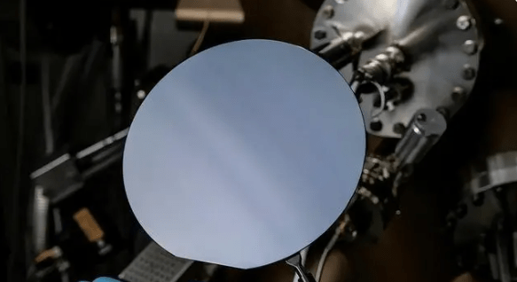
Gallium nitride is a kind of synthetic semiconductor material, which is a typical representative of the third generation of semiconductor materials. Compared with traditional silicon materials, gallium nitride (GaN) has the advantages of large band-gap, strong breakdown electric field, low on-resistance, high electron mobility, high conversion efficiency, high thermal conductivity and low loss.
Gallium nitride single crystal is a new generation of semiconductor materials with excellent performance, which can be widely used in communication, radar, consumer electronics, automotive electronics, power energy, industrial laser processing, instrumentation and other fields, so its development and mass production are the focus of attention of countries and industries around the world.
Application of GaN
1--5G communication base station
Wireless communication infrastructure is the main application area of gallium nitride RF devices, accounting for 50%.
2--High power supply
The "double height" feature of GaN has great penetration potential in high-performance consumer electronic devices, which can meet the requirements of fast charging and charge protection scenarios.
3--New energy vehicle
From the practical application point of view, the current third-generation semiconductor devices on the car are mainly silicon carbide devices, but there are suitable gallium nitride materials that can pass the car regulation certification of power device modules, or other suitable packaging methods, will still be accepted by the whole plant and OEM manufacturers.
4--Data center
GaN power semiconductors are mainly used in PSU power supply units in data centers.
In summary, with the outbreak of new downstream applications and continuous breakthroughs in gallium nitride substrate preparation technology, GaN devices are expected to continue to increase in volume, and will become one of the key technologies for cost reduction and efficiency and sustainable green development.
Post time: Jul-27-2023