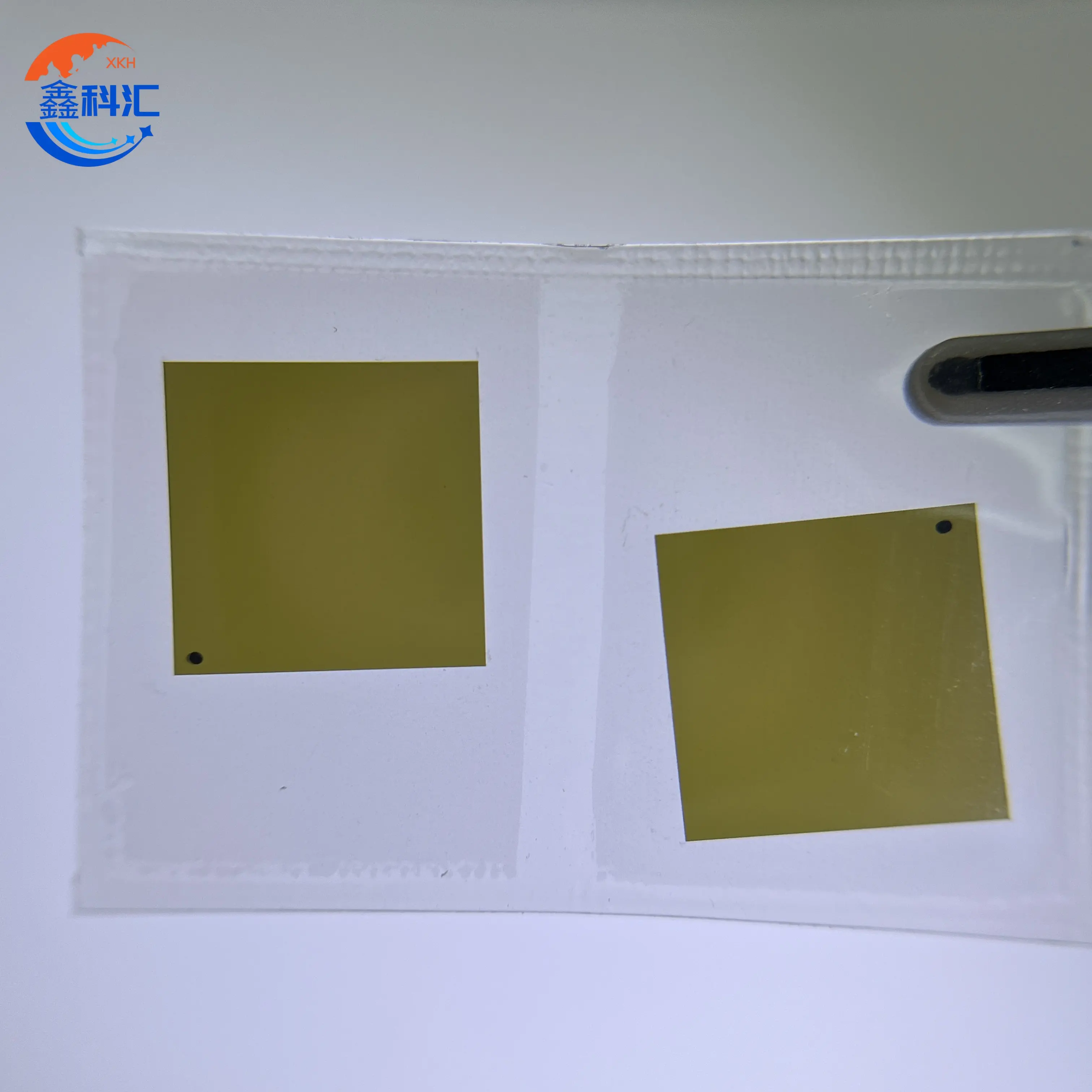
Silicon carbide (SiC), as a third-generation semiconductor material, is gaining significant attention due to its superior physical properties and promising applications in high-power electronics. Unlike traditional silicon (Si) or germanium (Ge) semiconductors, SiC possesses a wide bandgap, high thermal conductivity, high breakdown field, and excellent chemical stability. These characteristics make SiC an ideal material for power devices in electric vehicles, renewable energy systems, 5G communications, and other high-efficiency, high-reliability applications. However, despite its potential, the SiC industry faces profound technical challenges that constitute significant barriers to widespread adoption.
1. SiC Substrate: Crystal Growth and Wafer Fabrication
The production of SiC substrates is the foundation of the SiC industry and represents the highest technical barrier. SiC cannot be grown from the liquid phase like silicon due to its high melting point and complex crystal chemistry. Instead, the primary method is physical vapor transport (PVT), which involves sublimating high-purity silicon and carbon powders at temperatures exceeding 2000°C in a controlled environment. The growth process requires precise control over temperature gradients, gas pressure, and flow dynamics to produce high-quality single crystals.
SiC has over 200 polytypes, but only a few are suitable for semiconductor applications. Ensuring the correct polytype while minimizing defects such as micropipes and threading dislocations is critical, as these defects severely affect device reliability. The slow growth rate, often less than 2 mm per hour, results in crystal growth times of up to a week for a single boule, compared to just a few days for silicon crystals.
After crystal growth, the processes of slicing, grinding, polishing, and cleaning are exceptionally challenging due to SiC’s hardness, second only to diamond. These steps must preserve surface integrity while avoiding microcracks, edge chipping, and subsurface damage. As wafer diameters increase from 4 inches to 6 or even 8 inches, controlling thermal stress and achieving defect-free expansion becomes increasingly complex.
2. SiC Epitaxy: Layer Uniformity and Doping Control
Epitaxial growth of SiC layers on substrates is crucial because the device’s electrical performance directly depends on the quality of these layers. Chemical vapor deposition (CVD) is the dominant method, allowing precise control over doping type (n-type or p-type) and layer thickness. As voltage ratings increase, the required epitaxial layer thickness can rise from a few micrometers to tens or even hundreds of micrometers. Maintaining uniform thickness, consistent resistivity, and low defect density across thick layers is extremely difficult.
Epitaxy equipment and processes are currently dominated by a few global suppliers, creating high entry barriers for new manufacturers. Even with high-quality substrates, poor epitaxial control can lead to low yield, reduced reliability, and suboptimal device performance.
3. Device Fabrication: Precision Processes and Material Compatibility
SiC device fabrication presents further challenges. Traditional silicon diffusion methods are ineffective due to SiC’s high melting point; ion implantation is used instead. High-temperature annealing is required to activate dopants, which risks crystal lattice damage or surface degradation.
The formation of high-quality metal contacts is another critical difficulty. Low contact resistance (<10⁻⁵ Ω·cm²) is essential for power device efficiency, yet typical metals such as Ni or Al have limited thermal stability. Composite metallization schemes improve stability but increase contact resistance, making optimization highly challenging.
SiC MOSFETs also suffer from interface issues; the SiC/SiO₂ interface often has a high density of traps, limiting channel mobility and threshold voltage stability. Rapid switching speeds further exacerbate issues with parasitic capacitance and inductance, demanding careful design of gate drive circuits and packaging solutions.
4. Packaging and System Integration
SiC power devices operate at higher voltages and temperatures than silicon counterparts, necessitating novel packaging strategies. Conventional wire-bonded modules are insufficient due to thermal and electrical performance limitations. Advanced packaging approaches, such as wireless interconnects, double-sided cooling, and integration of decoupling capacitors, sensors, and drive circuitry, are required to fully exploit SiC’s capabilities. Trench-type SiC devices with higher unit density are becoming the mainstream due to their lower conduction resistance, reduced parasitic capacitance, and improved switching efficiency.
5. Cost Structure and Industry Implications
The high cost of SiC devices is primarily due to substrate and epitaxial material production, which together account for roughly 70% of total manufacturing costs. Despite the high costs, SiC devices offer performance advantages over silicon, particularly in high-efficiency systems. As substrate and device production scales and yields improve, the cost is expected to decrease, making SiC devices more competitive in automotive, renewable energy, and industrial applications.
Conclusion
The SiC industry represents a major technological leap in semiconductor materials, but its adoption is constrained by complex crystal growth, epitaxial layer control, device fabrication, and packaging challenges. Overcoming these barriers requires precise temperature control, advanced materials processing, innovative device structures, and new packaging solutions. Continuous breakthroughs in these areas will not only reduce costs and improve yields but also unlock the full potential of SiC in next-generation power electronics, electric vehicles, renewable energy systems, and high-frequency communication applications.
The future of the SiC industry lies in the integration of material innovation, precision manufacturing, and device design, driving a shift from silicon-based solutions to high-efficiency, high-reliability wide-bandgap semiconductors.
Post time: Dec-10-2025

