1. From Silicon to Silicon Carbide: A Paradigm Shift in Power Electronics
For more than half a century, silicon has been the backbone of power electronics. However, as electric vehicles, renewable energy systems, AI data centers, and aerospace platforms push toward higher voltages, higher temperatures, and higher power densities, silicon is approaching its fundamental physical limits.
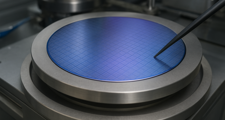
Silicon carbide (SiC), a wide-bandgap semiconductor with a bandgap of ~3.26 eV (4H-SiC), has emerged as a materials-level solution rather than a circuit-level workaround. Yet, the true performance advantage of SiC devices is not determined solely by the material itself, but by the purity of the SiC wafer on which devices are built.
In next-generation power electronics, high-purity SiC wafers are not a luxury—they are a necessity.
2. What “High Purity” Really Means in SiC Wafers
In the context of SiC wafers, purity extends far beyond chemical composition. It is a multidimensional materials parameter, including:
-
Ultra-low unintentional dopant concentration
-
Suppression of metallic impurities (Fe, Ni, V, Ti)
-
Control of intrinsic point defects (vacancies, antisites)
-
Reduction of extended crystallographic defects
Even trace impurities at the parts-per-billion (ppb) level can introduce deep energy levels in the bandgap, acting as carrier traps or leakage pathways. Unlike silicon, where impurity tolerance is relatively forgiving, SiC’s wide bandgap amplifies the electrical impact of every defect.
3. High Purity and the Physics of High-Voltage Operation
The defining advantage of SiC power devices lies in their ability to sustain extreme electric fields—up to ten times higher than silicon. This capability depends critically on uniform electric field distribution, which in turn requires:
-
Highly homogeneous resistivity
-
Stable and predictable carrier lifetime
-
Minimal deep-level trap density
Impurities disrupt this balance. They locally distort the electric field, leading to:
-
Premature breakdown
-
Increased leakage current
-
Reduced blocking voltage reliability
In ultra-high-voltage devices (≥1200 V, ≥1700 V), device failure often originates from a single impurity-induced defect, not from the average material quality.
4. Thermal Stability: Purity as an Invisible Heat Sink
SiC is renowned for its high thermal conductivity and ability to operate above 200 °C. However, impurities act as phonon scattering centers, degrading heat transport at the microscopic level.
High-purity SiC wafers enable:
-
Lower junction temperatures at the same power density
-
Reduced thermal runaway risk
-
Longer device lifetime under cyclic thermal stress
In practical terms, this means smaller cooling systems, lighter power modules, and higher system-level efficiency—key metrics in EVs and aerospace electronics.
5. High Purity and Device Yield: The Economics of Defects
As SiC manufacturing moves toward 8-inch and eventually 12-inch wafers, defect density scales non-linearly with wafer area. In this regime, purity becomes an economic variable, not just a technical one.
High-purity wafers deliver:
-
Higher epitaxial layer uniformity
-
Improved MOS interface quality
-
Significantly higher device yield per wafer
For manufacturers, this directly translates to lower cost per ampere, accelerating SiC’s adoption in cost-sensitive applications such as onboard chargers and industrial inverters.
6. Enabling the Next Wave: Beyond Conventional Power Devices
High-purity SiC wafers are not only critical for today’s MOSFETs and Schottky diodes. They are the enabling substrate for future architectures, including:
-
Ultra-fast solid-state circuit breakers
-
High-frequency power ICs for AI data centers
-
Radiation-hard power devices for space missions
-
Monolithic integration of power and sensing functions
These applications demand extreme material predictability, where purity is the foundation upon which advanced device physics can be reliably engineered.
7. Conclusion: Purity as a Strategic Technology Lever
In next-generation power electronics, performance gains no longer come primarily from clever circuit design. They originate one level deeper—at the atomic structure of the wafer itself.
High-purity SiC wafers transform silicon carbide from a promising material into a scalable, reliable, and economically viable platform for the electrified world. As voltage levels rise, system sizes shrink, and efficiency targets tighten, purity becomes the silent determinant of success.
In this sense, high-purity SiC wafers are not just components—they are strategic infrastructure for the future of power electronics.
Post time: Jan-07-2026