When examining semiconductor silicon wafers or substrates made of other materials, we often encounter technical indicators such as: TTV, BOW, WARP, and possibly TIR, STIR, LTV, among others. What parameters do these represent?
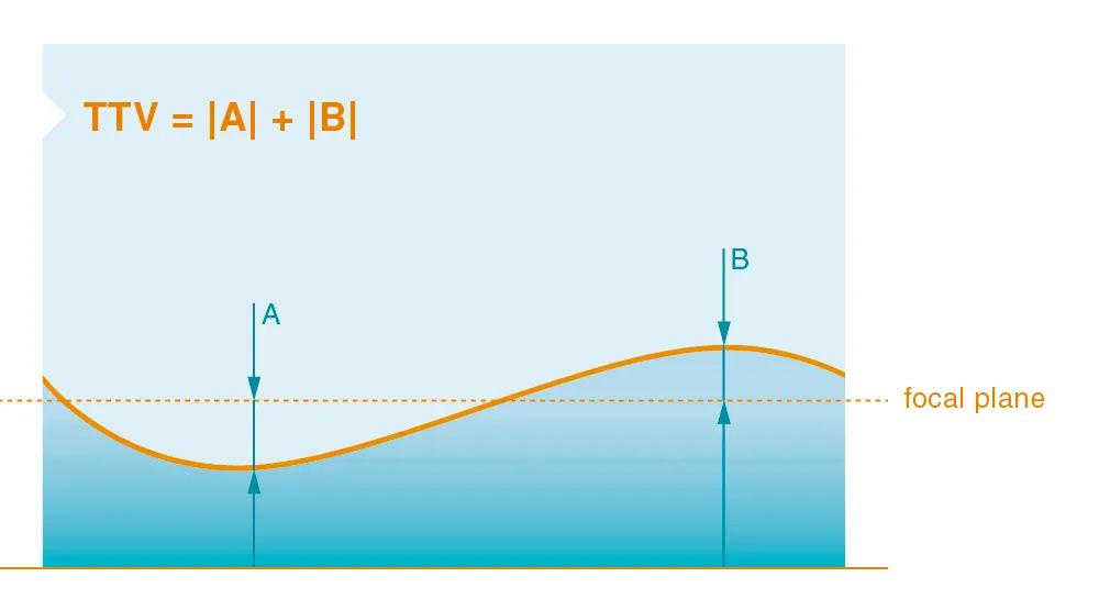
TTV — Total Thickness Variation
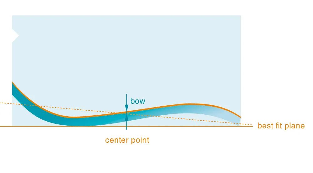
BOW — Bow
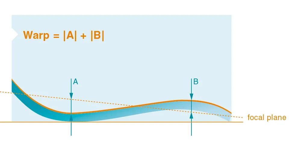
WARP — Warp
TIR — Total Indicated Reading
STIR — Site Total Indicated Reading
LTV — Local Thickness Variation
1. Total Thickness Variation — TTV
 The difference between the maximum and minimum thickness of the wafer relative to the reference plane when the wafer is clamped and in close contact. It is generally expressed in micrometers (μm), often represented as: ≤15 μm.
2. Bow — BOW
The deviation between the minimum and maximum distance from the center point of the wafer surface to the reference plane when the wafer is in a free (unclamped) state. This includes both concave (negative bow) and convex (positive bow) cases. It is typically expressed in micrometers (μm), often represented as: ≤40 μm.
3. Warp — WARP
The deviation between the minimum and maximum distance from the wafer surface to the reference plane (usually the back surface of the wafer) when the wafer is in a free (unclamped) state. This includes both concave (negative warp) and convex (positive warp) cases. It is generally expressed in micrometers (μm), often represented as: ≤30 μm.
4. Total Indicated Reading — TIR
When the wafer is clamped and in close contact, using a reference plane that minimizes the sum of intercepts of all points within the quality area or a specified local region on the wafer surface, the TIR is the deviation between the maximum and minimum distances from the wafer surface to this reference plane.
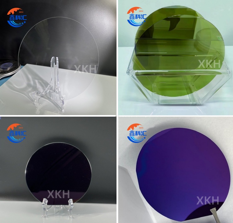
Founded on deep expertise in semiconductor material specifications such as TTV, BOW, WARP, and TIR, XKH provides precision custom wafer processing services tailored to stringent industry standards. We supply and support a wide range of high-performance materials including sapphire, silicon carbide (SiC), silicon wafers, SOI, and quartz, ensuring exceptional flatness, thickness consistency, and surface quality for advanced applications in optoelectronics, power devices, and MEMS. Trust us to deliver reliable material solutions and precision machining that meet your most demanding design requirements.
Post time: Aug-29-2025


