Directory
1. Core Concepts and Metrics
2. Measurement Techniques
3. Data Processing and Errors
4. Process Implications
In semiconductor manufacturing, the thickness uniformity and surface flatness of wafers are critical factors affecting process yield. Key parameters such as Total Thickness Variation (TTV), Bow (arcuate warpage), Warp (global warpage), and Microwarp (nano-topography) directly impact the precision and stability of core processes like photolithography focus, chemical mechanical polishing (CMP), and thin-film deposition.
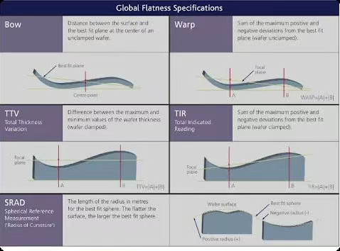
Core Concepts and Metrics
TTV (Total Thickness Variation)
Warp
Warp quantifies the maximum peak-to-valley difference across all surface points relative to the reference plane, evaluating the wafer’s overall flatness in a free state.
Measurement Techniques
1. TTV Measurement Methods
- Dual-Surface Profilometry
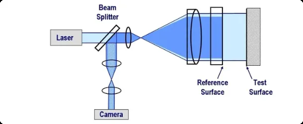
- Fizeau Interferometry: Uses interference fringes between a reference plane and the wafer surface. Suitable for smooth surfaces but limited by large-curvature wafers.
- White Light Scanning Interferometry (SWLI): Measures absolute heights via low-coherence light envelopes. Effective for step-like surfaces but constrained by mechanical scanning speed.
- Confocal Methods: Achieve sub-micron resolution via pinhole or dispersion principles. Ideal for rough or translucent surfaces but slow due to point-by-point scanning.
- Laser Triangulation: Rapid response but prone to accuracy loss from surface reflectivity variations.
- Transmission/Reflection Coupling
- Dual-Head Capacitance Sensors: Symmetric placement of sensors on both sides measures thickness as T = L – d₁ – d₂ (L = baseline distance). Fast but sensitive to material properties.
- Ellipsometry/Spectroscopic Reflectometry: Analyzes light-matter interactions for thin-film thickness but unsuitable for bulk TTV.
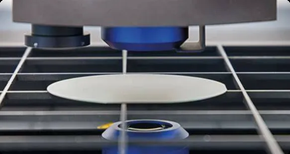
2. Bow and Warp Measurement
- Multi-Probe Capacitance Arrays: Capture full-field height data on an air-bearing stage for rapid 3D reconstruction.
- Structured Light Projection: High-speed 3D profiling using optical shaping.
- Low-NA Interferometry: High-resolution surface mapping but vibration-sensitive.
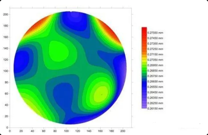
3. Microwarp Measurement
- Spatial Frequency Analysis:
- Acquire high-resolution surface topography.
- Compute power spectral density (PSD) via 2D FFT.
- Apply bandpass filters (e.g., 0.5–20 mm) to isolate critical wavelengths.
- Calculate RMS or P-V values from filtered data.
- Vacuum Chuck Simulation: Mimic real-world clamping effects during lithography.
Data Processing and Error Sources
Processing Workflow
- TTV: Align front/back surface coordinates, compute thickness difference, and subtract systematic errors (e.g., thermal drift).
- Bow/Warp: Fit LSQ plane to height data; Bow = center point residual, Warp = peak-to-valley residual.
- Microwarp: Filter spatial frequencies, compute statistics (RMS/P-V).
Key Error Sources
- Environmental Factors: Vibration (critical for interferometry), air turbulence, thermal drift.
- Sensor Limitations: Phase noise (interferometry), wavelength calibration errors (confocal), material-dependent responses (capacitance).
- Wafer Handling: Edge exclusion misalignment, motion stage inaccuracies in stitching.
Impact on Process Criticality
- Lithography: Local microwarp reduces DOF, causing CD variation and overlay errors.
- CMP: Initial TTV imbalance leads to non-uniform polishing pressure.
- Stress Analysis: Bow/Warp evolution reveals thermal/mechanical stress behavior.
- Packaging: Excessive TTV creates voids in bonding interfaces.
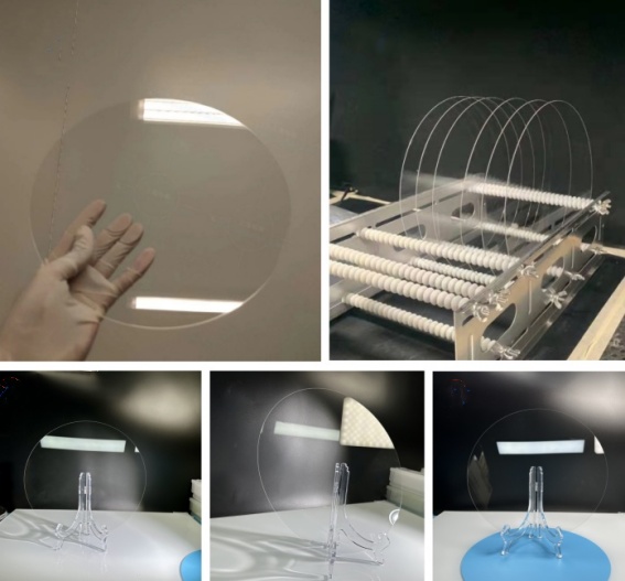
XKH‘s Sapphire Wafer
Post time: Sep-28-2025