Table of Contents
1. Technological Shift: The Rise of Silicon Carbide and Its Challenges
2. TSMC’s Strategic Shift: Exiting GaN and Betting on SiC
3. Material Competition: The Irreplaceability of SiC
4. Application Scenarios: The Thermal Management Revolution in AI Chips and Next-Gen Electronics
5. Future Challenges: Technical Bottlenecks and Industry Competition
According to TechNews, the global semiconductor industry has entered an era driven by artificial intelligence (AI) and high-performance computing (HPC), where thermal management has emerged as a core bottleneck impacting chip design and process breakthroughs. As advanced packaging architectures like 3D stacking and 2.5D integration continue to increase chip density and power consumption, traditional ceramic substrates can no longer meet thermal flux demands. TSMC, the world’s leading wafer foundry, is responding to this challenge with a bold material shift: fully embracing 12-inch single-crystal silicon carbide (SiC) substrates while gradually exiting the gallium nitride (GaN) business. This move not only signifies a recalibration of TSMC’s material strategy but also highlights how thermal management has transitioned from a “supporting technology” to a “core competitive advantage.”
Silicon Carbide: Beyond Power Electronics
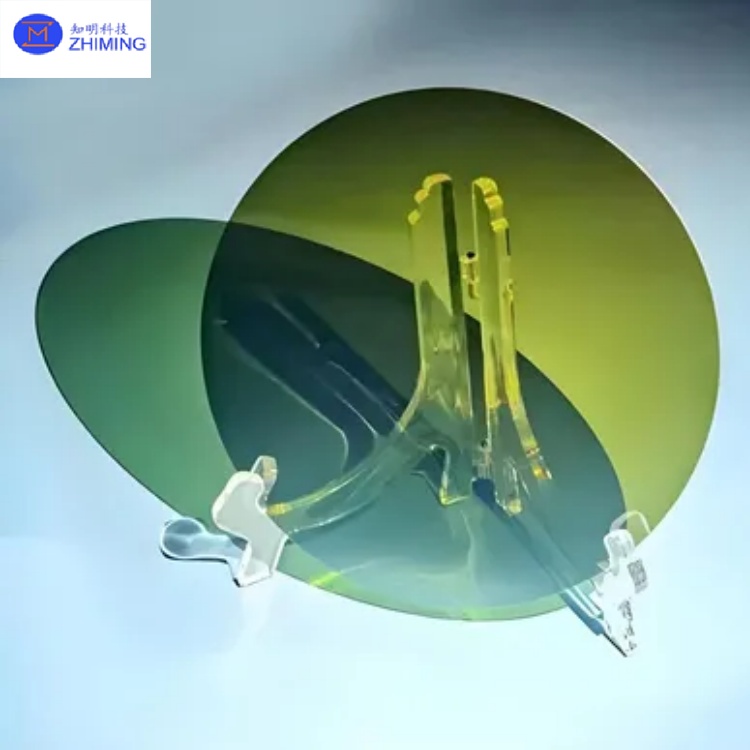
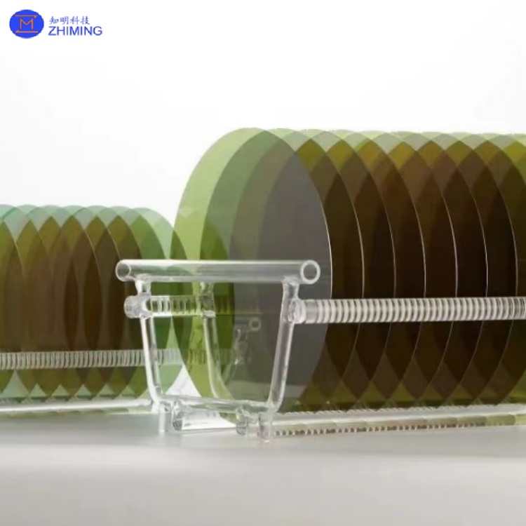
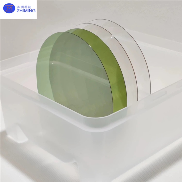
Silicon carbide, renowned for its wide bandgap semiconductor properties, has traditionally been used in high-efficiency power electronics such as electric vehicle inverters, industrial motor controls, and renewable energy infrastructure. However, SiC’s potential extends far beyond this. With an exceptional thermal conductivity of approximately 500 W/mK—far surpassing conventional ceramic substrates like aluminum oxide (Al₂O₃) or sapphire—SiC is now poised to address the escalating thermal challenges of high-density applications.
AI Accelerators and the Thermal Crisis
The proliferation of AI accelerators, data center processors, and AR smart glasses has intensified spatial constraints and thermal management dilemmas. In wearable devices, for instance, microchip components positioned near the eye demand precise thermal control to ensure safety and stability. Leveraging its decades of expertise in 12-inch wafer fabrication, TSMC is advancing large-area single-crystal SiC substrates to replace traditional ceramics. This strategy enables seamless integration into existing production lines, balancing yield and cost advantages without requiring a complete manufacturing overhaul.
Technical Challenges and Innovations
SiC’s Role in Advanced Packaging
- 2.5D Integration: Chips are mounted on silicon or organic interposers with short, efficient signal paths. Heat dissipation challenges here are primarily horizontal.
- 3D Integration: Vertically stacked chips via through-silicon vias (TSVs) or hybrid bonding achieve ultra-high interconnect density but face exponential thermal pressure. SiC not only serves as a passive thermal material but also synergizes with advanced solutions like diamond or liquid metal to form “hybrid cooling” systems.
Strategic Exit from GaN
Beyond Automotive: SiC’s New Frontiers
- Conductive N-type SiC: Acts as thermal spreaders in AI accelerators and high-performance processors.
- Insulating SiC: Serves as interposers in chiplet designs, balancing electrical isolation with thermal conduction.
These innovations position SiC as the foundational material for thermal management in AI and data center chips.
The Material Landscape
TSMC’s 12-inch wafer expertise differentiates it from competitors, enabling rapid deployment of SiC platforms. By leveraging existing infrastructure and advanced packaging technologies like CoWoS, TSMC aims to transform material advantages into system-level thermal solutions. Concurrently, industry giants like Intel are prioritizing backside power delivery and thermal-power co-design, underscoring the global shift toward thermal-centric innovation.
Post time: Sep-28-2025


