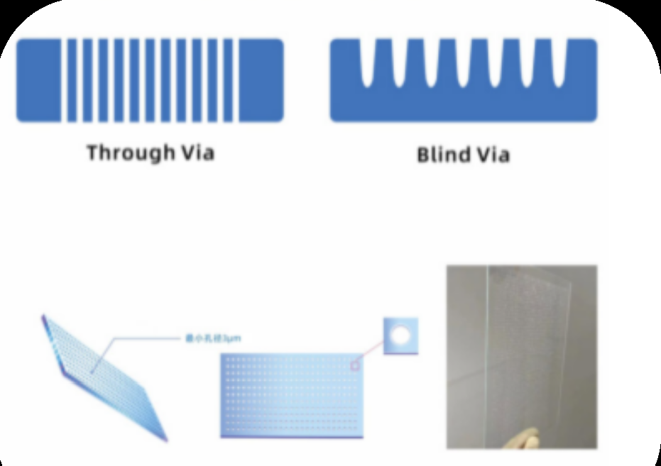
TGV (Through Glass Via) Process
TGV (Through Glass Via) is an advanced packaging technology that creates vertically through microvias in ultra-thin glass substrates and metallizes them to enable vertical interconnection between chips. Featuring low loss at high frequencies, low thermal stress, and cost advantages, TGV is regarded as one of the key solutions for 2.5D/3D packaging and Chiplet integration.
Core Principle
The TGV processinvolvesfabricating micron-scale through holes, typically10–50 μm in diameter, in 100–700 μm ultra-thin glass substrates such as borosilicate glass or quartz. These vias are then filled with copper by electroplating to form vertical conductive channels, serving as an alternative to traditional TSV silicon interposers.
StandardProcessFlow
1. Substrate Pretreatment
The glass substrate is cleaned, dried, and coated with photoresist, followed by photolithography to remove contaminants and define the viapatterns.
2. LaserViaFormation
This is the core step of the TGV process. An ultrafast laser, such as a picosecond or femtosecond laser, is focused inside the glass to induce microcracks or modifiedregions, forming high-aspect-ratioviachannels. The aspectratio can reach up to 150:1, with via diameters as small as 3 μm and hole-to-hole uniformity exceeding 95% across millions of vias.
3. Wet Etching / Via Enlargement / Cleaning
HF or BHF etching is used to remove the laser-modifiedregions, smooth the via sidewalls, and precisely control the final viadiameter. The substrate is then thoroughly cleaned to removeresidual impurities.
4. Metallization
Seed Layer Deposition:
A Ti/Cu or AlN/Cu seed layer is deposited by sputtering to ensure strong adhesion to the via sidewalls.
Copper Electroplating:
Pulse or DC electroplating is used to achieve complete, void-free copper filling inside the vias.
Surface Treatment:
CMP is performed to planarize the surface, followed by anti-oxidation coating if required.
5. RDL Formation / Bumping
A redistribution layer is fabricated with fine line/space capability, typically ≤2 μm, followed by solder ball placement or copper pillar formation for subsequent chip bonding.

6. Testing / Dicing
Electrical testing is performed, followed by wafer dicing and final product inspection.
Summary
With its advantages of high-frequency low-loss performance, low thermal stress, and competitive cost, TGV has become a key technology for 3D interconnection in the post-Moore era. Its core technical breakthroughs lie in laser via formation and void-free copper electroplating. As the technology moves toward mass production in 2026, it is expected to play an important role in AI computing, 5G/6G RF devices, advanced packaging, and Chiplet integration.
Post time: Jun-09-2026