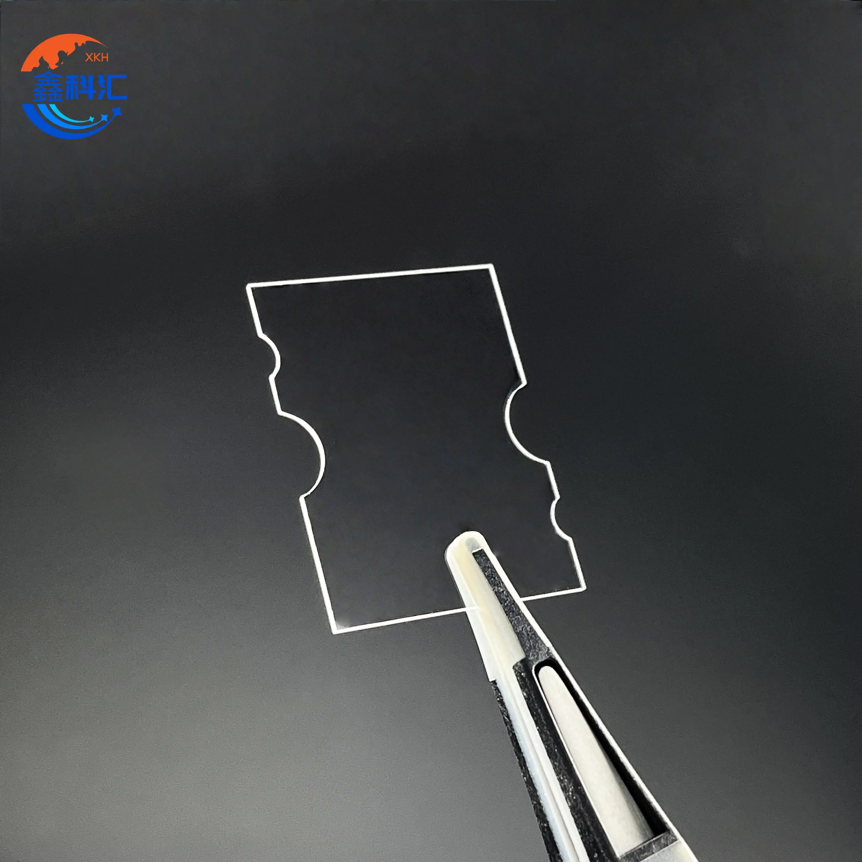
In the semiconductor industry, substrates are the foundational material on which device performance depends. Their physical, thermal, and electrical properties directly affect efficiency, reliability, and application scope. Among all options, sapphire (Al₂O₃), silicon (Si), and silicon carbide (SiC) have become the most widely used substrates, each excelling in different technology areas. This article explores their material characteristics, application landscapes, and future development trends.
Sapphire: The Optical Workhorse
Sapphire is a single-crystal form of aluminum oxide with a hexagonal lattice. Its key properties include exceptional hardness (Mohs hardness 9), broad optical transparency from ultraviolet to infrared, and strong chemical resistance, making it ideal for optoelectronic devices and harsh environments. Advanced growth techniques like Heat Exchange Method and Kyropoulos method, combined with chemical-mechanical polishing (CMP), produce wafers with sub-nanometer surface roughness.
Sapphire substrates are widely used in LEDs and Micro-LEDs as GaN epitaxial layers, where patterned sapphire substrates (PSS) improve light extraction efficiency. They are also used in high-frequency RF devices due to their electrical insulation properties, and in consumer electronics and aerospace applications as protective windows and sensor covers. Limitations include relatively low thermal conductivity (35–42 W/m·K) and lattice mismatch with GaN, which requires buffer layers to minimize defects.
Silicon: The Microelectronics Foundation
Silicon remains the backbone of traditional electronics due to its mature industrial ecosystem, adjustable electrical conductivity through doping, and moderate thermal properties (thermal conductivity ~150 W/m·K, melting point 1410°C). Over 90% of integrated circuits, including CPUs, memory, and logic devices, are fabricated on silicon wafers. Silicon also dominates photovoltaic cells and is widely used in low-to-medium power devices like IGBTs and MOSFETs.
However, silicon faces challenges in high-voltage and high-frequency applications due to its narrow bandgap (1.12 eV) and indirect bandgap, which limits light emission efficiency.
Silicon Carbide: The High-Power Innovator
SiC is a third-generation semiconductor material with a wide bandgap (3.2 eV), high breakdown voltage (3 MV/cm), high thermal conductivity (~490 W/m·K), and fast electron saturation velocity (~2×10⁷ cm/s). These characteristics make it ideal for high-voltage, high-power, and high-frequency devices. SiC substrates are typically grown via physical vapor transport (PVT) at temperatures exceeding 2000°C, with complex and precise processing requirements.
Applications include electric vehicles, where SiC MOSFETs improve inverter efficiency by 5–10%, 5G communication systems using semi-insulating SiC for GaN RF devices, and smart grids with high-voltage direct current (HVDC) transmission reducing energy losses by up to 30%. Limitations are high costs (6-inch wafers are 20–30 times more expensive than silicon) and processing challenges due to extreme hardness.
Complementary Roles and Future Outlook
Sapphire, silicon, and SiC form a complementary substrate ecosystem in the semiconductor industry. Sapphire dominates optoelectronics, silicon supports traditional microelectronics and low-to-medium power devices, and SiC leads high-voltage, high-frequency, and high-efficiency power electronics.
Future developments include expanding sapphire applications in deep-UV LEDs and micro-LEDs, enabling Si-based GaN heteroepitaxy to enhance high-frequency performance, and scaling SiC wafer production to 8 inches with improved yield and cost efficiency. Together, these materials are driving innovation across 5G, AI, and electric mobility, shaping the next generation of semiconductor technology.
Post time: Nov-24-2025

