The power semiconductor industry is undergoing a transformative shift driven by the rapid adoption of wide-bandgap (WBG) materials. Silicon Carbide (SiC) and Gallium Nitride (GaN) are at the forefront of this revolution, enabling next-generation power devices with higher efficiency, faster switching, and superior thermal performance. These materials are not only redefining the electrical characteristics of power semiconductors but also creating new challenges and opportunities in packaging technology. Effective packaging is critical to fully leverage the potential of SiC and GaN devices, ensuring reliability, performance, and longevity in demanding applications such as electric vehicles (EVs), renewable energy systems, and industrial power electronics.
The Advantages of SiC and GaN
Conventional silicon (Si) power devices have dominated the market for decades. However, as demand grows for higher power density, higher efficiency, and more compact form factors, silicon faces intrinsic limitations:
-
Limited breakdown voltage, making it challenging to operate safely at higher voltages.
-
Slower switching speeds, leading to increased switching losses in high-frequency applications.
-
Lower thermal conductivity, resulting in heat accumulation and stricter cooling requirements.
SiC and GaN, as WBG semiconductors, overcome these limitations:
-
SiC offers high breakdown voltage, excellent thermal conductivity (3–4 times that of silicon), and high-temperature tolerance, making it ideal for high-power applications like inverters and traction motors.
-
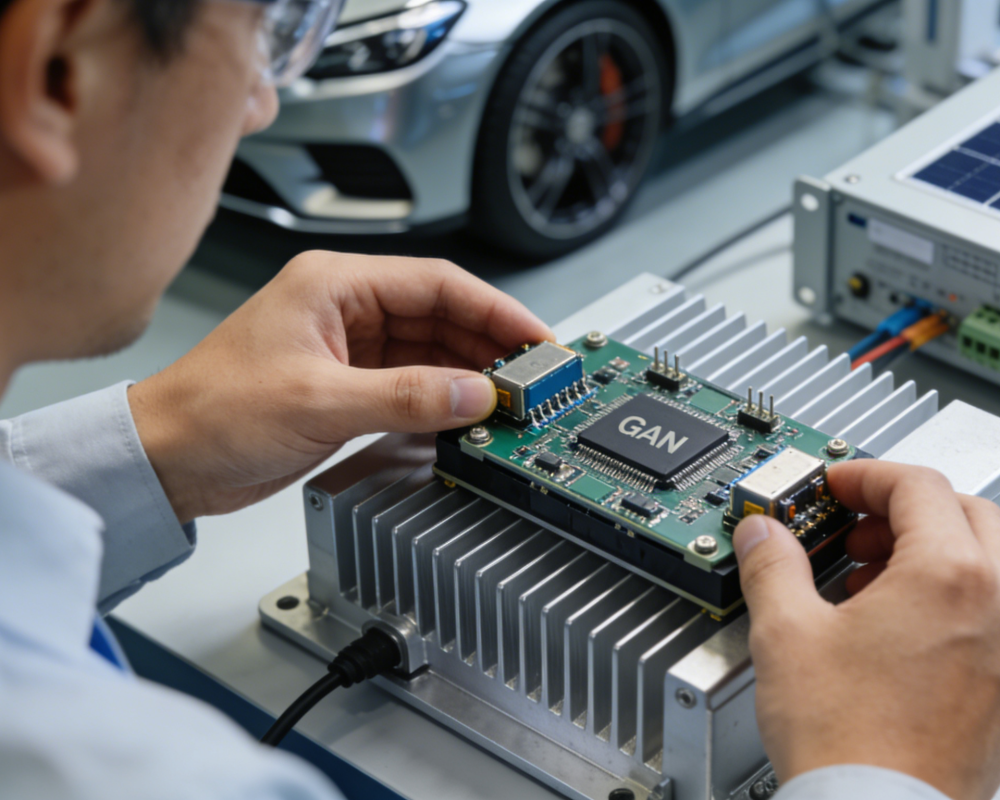
GaN provides ultra-fast switching, low on-resistance, and high electron mobility, enabling compact, high-efficiency power converters operating at high frequencies.
By leveraging these material advantages, engineers can design power systems with higher efficiency, smaller size, and improved reliability.
Implications for Power Packaging
While SiC and GaN improve device performance at the semiconductor level, packaging technology must evolve to address thermal, electrical, and mechanical challenges. Key considerations include:
-
Thermal Management
SiC devices can operate at temperatures exceeding 200°C. Efficient heat dissipation is critical to prevent thermal runaway and ensure long-term reliability. Advanced thermal interface materials (TIMs), copper-molybdenum substrates, and optimized heat-spreading designs are essential. Thermal considerations also influence die placement, module layout, and overall package size. -
Electrical Performance and Parasitics
GaN’s high switching speed makes package parasitics—such as inductance and capacitance—particularly critical. Even small parasitic elements can lead to voltage overshoot, electromagnetic interference (EMI), and switching losses. Packaging strategies such as flip-chip bonding, short current loops, and embedded die configurations are increasingly adopted to minimize parasitic effects. -
Mechanical Reliability
SiC is inherently brittle, and GaN-on-Si devices are sensitive to stress. Packaging must address thermal expansion mismatches, warpage, and mechanical fatigue to maintain device integrity under repeated thermal and electrical cycling. Low-stress die attach materials, compliant substrates, and robust underfills help mitigate these risks. -
Miniaturization and Integration
WBG devices enable higher power density, which drives demand for smaller packages. Advanced packaging techniques—such as chip-on-board (CoB), dual-sided cooling, and system-in-package (SiP) integration—allow designers to reduce footprint while maintaining performance and thermal control. Miniaturization also supports higher-frequency operation and faster response in power electronics systems.
Emerging Packaging Solutions
Several innovative packaging approaches have emerged to support SiC and GaN adoption:
-
Direct Bonded Copper (DBC) Substrates for SiC: DBC technology improves heat spreading and mechanical stability under high currents.
-
Embedded GaN-on-Si Designs: These reduce parasitic inductance and enable ultra-fast switching in compact modules.
-
High Thermal Conductivity Encapsulation: Advanced molding compounds and low-stress underfills prevent cracking and delamination under thermal cycling.
-
3D and Multi-Chip Modules: Integration of drivers, sensors, and power devices into a single package improves system-level performance and reduces board space.
These innovations highlight the critical role of packaging in unlocking the full potential of WBG semiconductors.
Conclusion
SiC and GaN are fundamentally transforming power semiconductor technology. Their superior electrical and thermal properties enable devices that are faster, more efficient, and capable of operating in harsher environments. However, realizing these benefits requires equally advanced packaging strategies that address thermal management, electrical performance, mechanical reliability, and miniaturization. Companies that innovate in SiC and GaN packaging will lead the next generation of power electronics, supporting energy-efficient and high-performance systems across automotive, industrial, and renewable energy sectors.
In summary, the revolution in power semiconductor packaging is inseparable from the rise of SiC and GaN. As the industry continues to push toward higher efficiency, higher density, and higher reliability, packaging will play a pivotal role in translating the theoretical advantages of wide-bandgap semiconductors into practical, deployable solutions.
Post time: Jan-14-2026