Silicon carbide (SiC) is not only a critical technology for national defense but also a pivotal material for global automotive and energy industries. As the first critical step in SiC single-crystal processing, wafer slicing directly determines the quality of subsequent thinning and polishing. Traditional slicing methods often introduce surface and subsurface cracks, increasing wafer breakage rates and manufacturing costs. Therefore, controlling surface crack damage is vital for advancing SiC device manufacturing.
Currently, SiC ingot slicing faces two major challenges:
- High material loss in traditional multi-wire sawing:SiC’s extreme hardness and brittleness make it prone to warping and cracking during cutting, grinding, and polishing. According to Infineon data, traditional reciprocating diamond-resin-bonded multi-wire sawing achieves only 50% material utilization in cutting, with total single-wafer loss reaching ~250 μm after polishing, leaving minimal usable material.
- Low efficiency and long production cycles:International production statistics show that producing 10,000 wafers using 24-hour continuous multi-wire sawing takes ~273 days. This method requires extensive equipment and consumables while generating high surface roughness and pollution (dust, wastewater).
To address these issues, Professor Xiu Xiangqian’s team at Nanjing University has developed high-precision laser slicing equipment for SiC, leveraging ultrafast laser technology to minimize defects and boost productivity. For a 20-mm SiC ingot, this technology doubles the wafer yield compared to traditional wire sawing. Additionally, the laser-sliced wafers exhibit superior geometric uniformity, enabling thickness reduction to 200 μm per wafer and further increasing output.
Key Advantages:
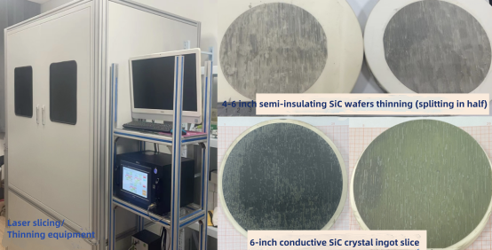
- Completed R&D on large-scale prototype equipment, validated for slicing 4–6-inch semi-insulating SiC wafers and 6-inch conductive SiC ingots.
- 8-inch ingot slicing is under verification.
- Significantly shorter slicing time, higher annual output, and >50% yield improvement.
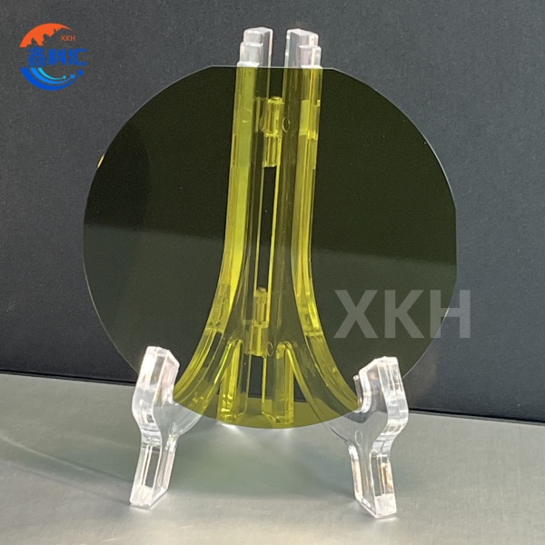
XKH’s SiC substrate of type 4H-N
Market Potential:
This equipment is poised to become the core solution for 8-inch SiC ingot slicing, currently dominated by Japanese imports with high costs and export restrictions. Domestic demand for laser slicing/thinning equipment exceeds 1,000 units, yet no mature Chinese-made alternatives exist. Nanjing University’s technology holds immense market value and economic potential.
Multi-Material Compatibility:
Beyond SiC, the equipment supports laser processing of gallium nitride (GaN), aluminum oxide (Al₂O₃), and diamond, broadening its industrial applications.
By revolutionizing SiC wafer processing, this innovation addresses critical bottlenecks in semiconductor manufacturing while aligning with global trends toward high-performance, energy-efficient materials.
Conclusion
As an industry leader in silicon carbide (SiC) substrate manufacturing, XKH specializes in providing 2-12-inch full-size SiC substrates (including 4H-N/SEMI-type, 4H/6H/3C-type) tailored to high-growth sectors such as new energy vehicles (NEVs), photovoltaic (PV) energy storage, and 5G communications. Leveraging large-dimension wafer low-loss slicing technology and high-precision processing technology, we have achieved mass production of 8-inch substrates and breakthroughs in 12-inch conductive SiC crystal growth technology, significantly reducing per-unit chip costs. Moving forward, we will continue to optimize ingot-level laser slicing and intelligent stress control processes to elevate 12-inch substrate yield to globally competitive levels, empowering the domestic SiC industry to break international monopolies and accelerate scalable applications in high-end domains like automotive-grade chips and AI server power supplies.
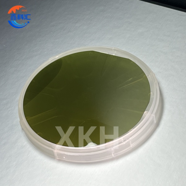
XKH’s SiC substrate of type 4H-N
Post time: Aug-15-2025