1. Introduction
Despite decades of research, heteroepitaxial 3C-SiC grown on silicon substrates has not yet achieved sufficient crystal quality for industrial electronic applications. Growth is typically performed on Si(100) or Si(111) substrates, each presenting distinct challenges: anti-phase domains for (100) and cracking for (111). While [111]-oriented films exhibit promising characteristics such as reduced defect density, improved surface morphology, and lower stress, alternative orientations like (110) and (211) remain understudied. Existing data suggest that optimal growth conditions may be orientation-specific, complicating systematic investigation. Notably, the use of higher-Miller-index Si substrates (e.g., (311), (510)) for 3C-SiC heteroepitaxy has never been reported, leaving significant room for exploratory research on orientation-dependent growth mechanisms.
2. Experimental
The 3C-SiC layers were deposited via atmospheric-pressure chemical vapor deposition (CVD) using SiH4/C3H8/H2 precursor gases. The substrates were 1 cm² Si wafers with various orientations: (100), (111), (110), (211), (311), (331), (510), (553), and (995). All substrates were on-axis except for (100), where 2° off-cut wafers were additionally tested. Pre-growth cleaning involved ultrasonic degreasing in methanol. The growth protocol comprised native oxide removal through H2 annealing at 1000°C, followed by a standard two-step process: carburization for 10 minutes at 1165°C with 12 sccm C3H8, then epitaxy for 60 minutes at 1350°C (C/Si ratio = 4) using 1.5 sccm SiH4 and 2 sccm C3H8. Each growth run included four to five different Si orientations, with at least one (100) reference wafer.
3. Results and Discussion
The morphology of 3C-SiC layers grown on various Si substrates (Fig. 1) showed distinct surface features and roughness. Visually, samples grown on Si(100), (211), (311), (553), and (995) appeared mirror-like, while others ranged from milky ((331), (510)) to dull ((110), (111)). The smoothest surfaces (showing the finest microstructure) were obtained on (100)2° off and (995) substrates. Remarkably, all layers remained crack-free after cooling, including the typically stress-prone 3C-SiC(111). The limited sample size may have prevented cracking, though some samples exhibited bowing (30-60 μm deflection from center to edge) detectable under optical microscopy at 1000× magnification due to accumulated thermal stress. Highly bowed layers grown on Si(111), (211), and (553) substrates displayed concave shapes indicating tensile strain, requiring further experimental and theoretical work to correlate with crystallographic orientation.
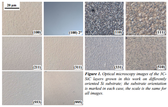
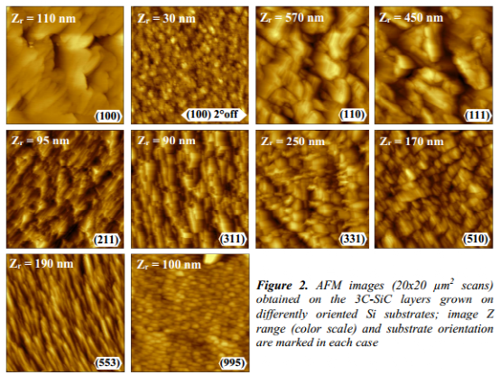
Figure 1 summarizes the XRD and AFM (scanning at 20×20 μ m2) results of the 3C-SC layers grown on Si substrates with different orientations.
Atomic force microscopy (AFM) images (Fig. 2) corroborated optical observations. Root-mean-square (RMS) values confirmed the smoothest surfaces on (100)2° off and (995) substrates, featuring grain-like structures with 400-800 nm lateral dimensions. The (110)-grown layer was the roughest, while elongated and/or parallel features with occasional sharp boundaries appeared in other orientations ((331), (510)). X-ray diffraction (XRD) θ-2θ scans (summarized in Table 1) revealed successful heteroepitaxy for lower-Miller-index substrates, except for Si(110) which showed mixed 3C-SiC(111) and (110) peaks indicating polycrystallinity. This orientation mixing has been previously reported for Si(110), though some studies observed exclusive (111)-oriented 3C-SiC, suggesting growth condition optimization is critical. For Miller indices ≥5 ((510), (553), (995)), no XRD peaks were detected in standard θ-2θ configuration since these high-index planes are non-diffracting in this geometry. The absence of low-index 3C-SiC peaks (e.g., (111), (200)) suggests single-crystalline growth, requiring sample tilting to detect diffraction from low-index planes.
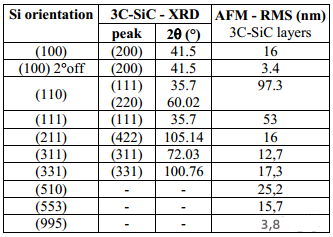
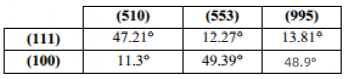
Figure 2 shows the calculation of the plane angle within the CFC crystal structure.
The calculated crystallographic angles between high-index and low-index planes (Table 2) showed large misorientations (>10°), explaining their absence in standard θ-2θ scans. Pole figure analysis was therefore conducted on the (995)-oriented sample due to its unusual granular morphology (potentially from columnar growth or twinning) and low roughness. The (111) pole figures (Fig. 3) from Si substrate and 3C-SiC layer were nearly identical, confirming epitaxial growth without twinning. The central spot appeared at χ≈15°, matching the theoretical (111)-(995) angle. Three symmetry-equivalent spots appeared at expected positions (χ=56.2°/φ=269.4°, χ=79°/φ=146.7° and 33.6°), though an unpredicted weak spot at χ=62°/φ=93.3° requires further investigation. The crystalline quality, assessed via spot width in φ-scans, appears promising, though rocking curve measurements are needed for quantification. Pole figures for (510) and (553) samples remain to be completed to confirm their presumed epitaxial nature.
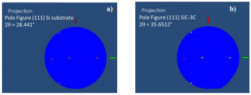
Figure 3 shows the XRD peak diagram recorded on the (995) oriented sample, which displays the (111) planes of the Si substrate (a) and the 3C-SiC layer (b).
4. Conclusion
Heteroepitaxial 3C-SiC growth succeeded on most Si orientations except (110), which yielded polycrystalline material. Si(100)2° off and (995) substrates produced the smoothest layers (RMS <1 nm), while (111), (211), and (553) showed significant bowing (30-60 μm). High-index substrates require advanced XRD characterization (e.g., pole figures) to confirm epitaxy due to absent θ-2θ peaks. Ongoing work includes rocking curve measurements, Raman stress analysis, and expansion to additional high-index orientations to complete this exploratory study.
As a vertically integrated manufacturer, XKH provide professional customized processing services with a comprehensive portfolio of silicon carbide substrates, offering standard and specialized types including 4H/6H-N, 4H-Semi, 4H/6H-P, and 3C-SiC, available in diameters from 2-inch to 12-inch. Our end-to-end expertise in crystal growth, precision machining, and quality assurance ensures tailored solutions for power electronics, RF, and emerging applications.
Post time: Aug-08-2025