FOUP stands for Front-Opening Unified Pod, a standardized container used in modern semiconductor manufacturing to transport and store wafers safely. As wafer sizes have increased, and fabrication processes have become more sensitive, maintaining a clean and controlled environment for wafers has become crucial. FOUPs are designed to meet these requirements, ensuring wafers are protected from dust, humidity, and mechanical damage during handling and storage.
FOUP Full Form and Variations
The full form of FOUP highlights its purpose: a container that opens from the front, allowing automated wafer handling tools to load and unload wafers without exposing them to the external environment. Variations such as FOUP None refer to situations where wafers are temporarily stored or transported without a FOUP, often in controlled internal environments. Understanding these distinctions is essential for engineers working with semiconductor equipment and wafer logistics.
Why FOUPs Are Critical in Semiconductor Manufacturing
Semiconductor fabrication involves hundreds of precise steps, from lithography and etching to deposition and testing. During these processes, wafers must be moved between tools without contamination. FOUPs provide a reliable solution by maintaining a controlled atmosphere, minimizing particle contamination, and allowing automated equipment to handle wafers consistently. The use of FOUPs improves yield, reduces defect rates, and ensures repeatable manufacturing quality across large-scale production lines.
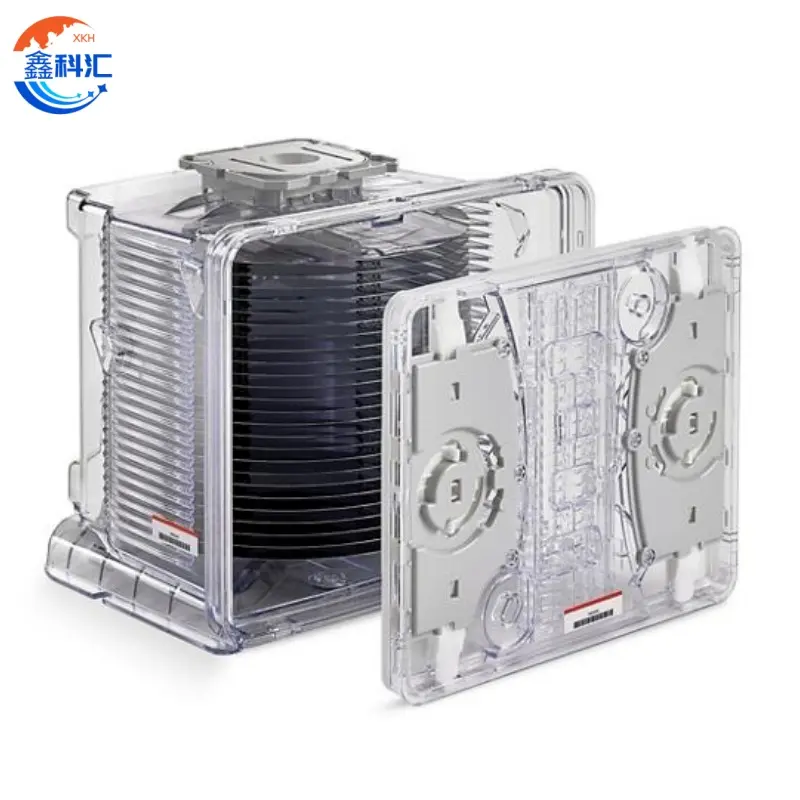
Design and Features of FOUPs
Modern FOUPs are typically made of durable, cleanroom-compatible plastics with precision-engineered slots to hold wafers securely. They often include features such as pressure relief valves, humidity control, and identification chips compatible with factory automation systems. The front-opening design is particularly suited for robotic handling, allowing equipment to access wafers without manual intervention. For engineers, knowing the specific FOUP type and configuration is essential when integrating new tools or upgrading production lines.
FOUP None in Practice
FOUP None situations occur in specialized manufacturing setups where wafers may be handled in batches or temporarily stored in intermediate carriers. While these setups still require strict environmental controls, they can be more flexible for research labs or pilot production lines. Engineers must understand the limitations and risks associated with using non-FOUP storage to ensure wafer integrity is maintained.
Choosing the Right FOUP for Your Facility
Selecting the appropriate FOUP depends on several factors, including wafer size, automation compatibility, environmental control requirements, and the specific processes involved. For large-scale fabs, standardized FOUPs for 300mm wafers are common, while smaller or experimental facilities may use customized carriers. Knowledge of FOUP specifications, handling protocols, and automation interfaces is essential to optimize wafer throughput and minimize contamination.
Conclusion
FOUPs play a vital role in modern semiconductor manufacturing, providing a standardized, safe, and automated method to transport and store wafers. Understanding the full form, variations, and practical applications of FOUPs, including FOUP None scenarios, is critical for engineers managing wafer logistics, automation, and production quality. By mastering these concepts, semiconductor professionals can ensure higher yields, better device reliability, and smoother production workflows.
Post time: Jan-09-2026