In the world of semiconductors, wafers are often called the “heart” of electronic devices. But a heart alone doesn’t make a living organism—protecting it, ensuring efficient operation, and connecting it seamlessly to the outside world require advanced packaging solutions. Let’s explore the fascinating world of wafer packaging in a way that’s both informative and easy to understand.
1. What is Wafer Packaging?
Simply put, wafer packaging is the process of “boxing up” a semiconductor chip to protect it and enable proper functionality. Packaging is not just about protection—it’s also a performance booster. Think of it like setting a gemstone in a fine piece of jewelry: it both protects and enhances the value.
Key purposes of wafer packaging include:
-
Physical Protection: Preventing mechanical damage and contamination
-
Electrical Connectivity: Ensuring stable signal paths for chip operation
-
Thermal Management: Helping chips dissipate heat efficiently
-
Reliability Enhancement: Maintaining stable performance under challenging conditions
2. Common Advanced Packaging Types
As chips become smaller and more complex, traditional packaging is no longer enough. This has led to the rise of several advanced packaging solutions:
2.5D Packaging
Multiple chips are interconnected through an intermediate silicon layer called an interposer.
Advantage: Improves communication speed between chips and reduces signal delay.
Applications: High-performance computing, GPUs, AI chips.
3D Packaging
Chips are stacked vertically and connected using TSV (Through-Silicon Vias).
Advantage: Saves space and increases performance density.
Applications: Memory chips, high-end processors.
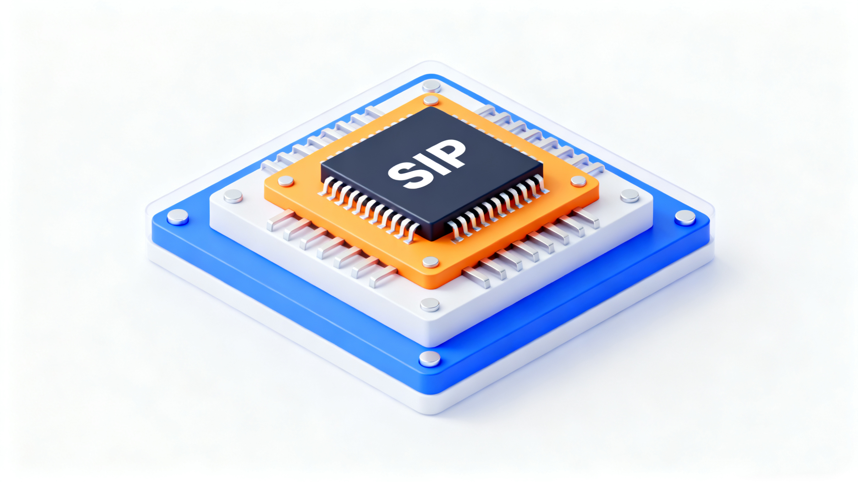
System-in-Package (SiP)
Multiple functional modules are integrated into a single package.
Advantage: Achieves high integration and reduces device size.
Applications: Smartphones, wearable devices, IoT modules.
Chip-Scale Packaging (CSP)
The package size is nearly the same as the bare chip.
Advantage: Ultra-compact and efficient connection.
Applications: Mobile devices, micro sensors.
3. Future Trends in Advanced Packaging
-
Smarter Thermal Management: As chip power increases, packaging needs to “breathe.” Advanced materials and microchannel cooling are emerging solutions.
-
Higher Functional Integration: Beyond processors, more components like sensors and memory are being integrated into a single package.
-
AI and High-Performance Applications: Next-generation packaging supports ultra-fast computation and AI workloads with minimal latency.
-
Sustainability: New packaging materials and processes are focusing on recyclability and lower environmental impact.
Advanced packaging is no longer just a supporting technology—it is a key enabler for the next generation of electronics, from smartphones to high-performance computing and AI chips. Understanding these solutions can help engineers, designers, and business leaders make smarter decisions for their projects.
Post time: Nov-12-2025