In semiconductor manufacturing, while photolithography and etching are the most frequently mentioned processes, epitaxial or thin film deposition techniques are equally critical. This article introduces several common thin film deposition methods used in chip fabrication, including MOCVD, magnetron sputtering, and PECVD.
Why Are Thin Film Processes Essential in Chip Manufacturing?
To illustrate, imagine a plain baked flatbread. On its own, it might taste bland. However, by brushing the surface with different sauces—like a savory bean paste or sweet malt syrup—you can completely transform its flavor. These flavor-enhancing coatings are akin to thin films in semiconductor processes, while the flatbread itself represents the substrate.
In chip fabrication, thin films serve numerous functional roles—insulation, conductivity, passivation, light absorption, etc.—and each function requires a specific deposition technique.
1. Metal-Organic Chemical Vapor Deposition (MOCVD)
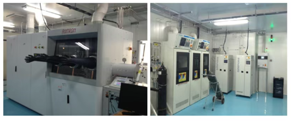
MOCVD is a highly advanced and precise technique used for the deposition of high-quality semiconductor thin films and nanostructures. It plays a crucial role in the fabrication of devices like LEDs, lasers, and power electronics.
Key Components of a MOCVD System:
- Gas Delivery System
Responsible for the precise introduction of reactants into the reaction chamber. This includes flow control of:
-
Carrier gases
-
Metal-organic precursors
-
Hydride gases
The system features multi-way valves for switching between growth and purge modes.
-
Reaction Chamber
The heart of the system where actual material growth occurs. Components include:-
Graphite susceptor (substrate holder)
-
Heater and temperature sensors
-
Optical ports for in-situ monitoring
-
Robotic arms for automated wafer loading/unloading
-
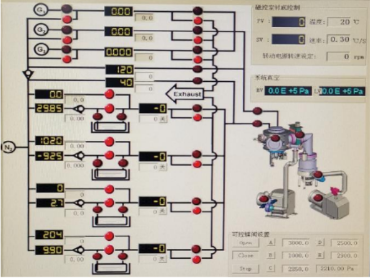
- Growth Control System
Consists of programmable logic controllers and a host computer. These ensure precise monitoring and repeatability throughout the deposition process. -
In-situ Monitoring
Tools such as pyrometers and reflectometers measure:-
Film thickness
-
Surface temperature
-
Substrate curvature
These enable real-time feedback and adjustment.
-
- Exhaust Treatment System
Treats toxic byproducts using thermal decomposition or chemical catalysis to ensure safety and environmental compliance.
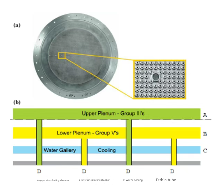
Closed-Coupled Showerhead (CCS) Configuration:
In vertical MOCVD reactors, the CCS design allows gases to be uniformly injected through alternating nozzles in a showerhead structure. This minimizes premature reactions and enhances uniform mixing.
-
The rotating graphite susceptor further helps homogenize the boundary layer of gases, improving film uniformity across the wafer.
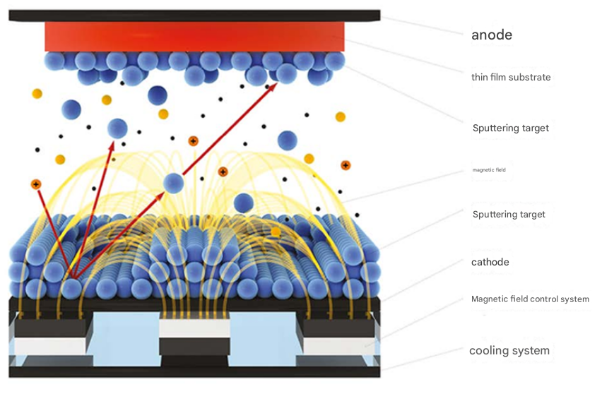
2. Magnetron Sputtering
Magnetron sputtering is a physical vapor deposition (PVD) method used widely for depositing thin films and coatings, particularly in electronics, optics, and ceramics.
Working Principle:
-
Target Material
The source material to be deposited—metal, oxide, nitride, etc.—is fixed on a cathode. -
Vacuum Chamber
The process is performed under high vacuum to avoid contamination. -
Plasma Generation
An inert gas, typically argon, is ionized to form plasma. -
Magnetic Field Application
A magnetic field confines electrons near the target to enhance ionization efficiency. -
Sputtering Process
Ions bombard the target, dislodging atoms that travel through the chamber and deposit onto the substrate.
Advantages of Magnetron Sputtering:
-
Uniform Film Deposition across large areas.
-
Capability to Deposit Complex Compounds, including alloys and ceramics.
-
Tunable Process Parameters for precise control of thickness, composition, and microstructure.
-
High Film Quality with strong adhesion and mechanical strength.
-
Broad Material Compatibility, from metals to oxides and nitrides.
-
Low-Temperature Operation, suitable for temperature-sensitive substrates.
3. Plasma-Enhanced Chemical Vapor Deposition (PECVD)
PECVD is widely used for the deposition of thin films like silicon nitride (SiNx), silicon dioxide (SiO₂), and amorphous silicon.
Principle:
In a PECVD system, precursor gases are introduced into a vacuum chamber where a glow discharge plasma is generated using:
-
RF excitation
-
DC high voltage
-
Microwave or pulsed sources
The plasma activates the gas-phase reactions, generating reactive species that deposit on the substrate to form a thin film.
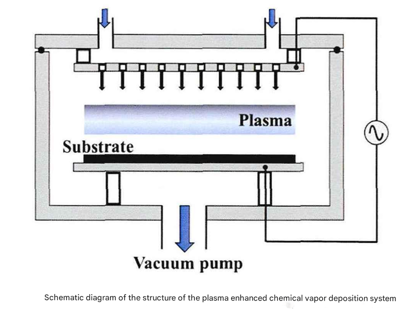
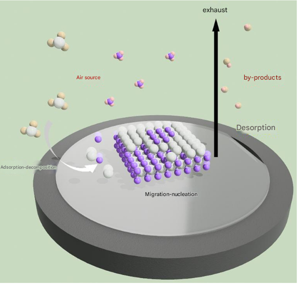
Deposition Steps:
-
Plasma Formation
Excited by electromagnetic fields, precursor gases ionize to form reactive radicals and ions. -
Reaction and Transport
These species undergo secondary reactions as they move toward the substrate. -
Surface Reaction
Upon reaching the substrate, they adsorb, react, and form a solid film. Some by-products are released as gases.
PECVD Benefits:
-
Excellent Uniformity in film composition and thickness.
-
Strong Adhesion even at relatively low deposition temperatures.
-
High Deposition Rates, making it suitable for industrial-scale production.
4. Thin Film Characterization Techniques
Understanding the properties of thin films is essential for quality control. Common techniques include:
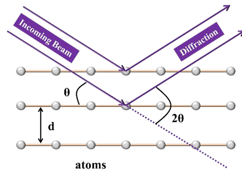
(1) X-ray Diffraction (XRD)
-
Purpose: Analyze crystal structures, lattice constants, and orientations.
-
Principle: Based on Bragg’s Law, measures how X-rays diffract through a crystalline material.
-
Applications: Crystallography, phase analysis, strain measurement, and thin film evaluation.
(2) Scanning Electron Microscopy (SEM)
-
Purpose: Observe surface morphology and microstructure.
-
Principle: Uses an electron beam to scan the sample surface. Detected signals (e.g., secondary and backscattered electrons) reveal surface details.
-
Applications: Materials science, nanotech, biology, and failure analysis.
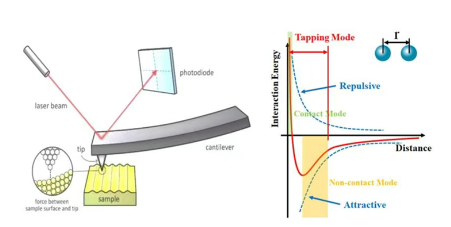
(3) Atomic Force Microscopy (AFM)
-
Purpose: Image surfaces at atomic or nanometer resolution.
-
Principle: A sharp probe scans the surface while maintaining constant interaction force; vertical displacements generate a 3D topography.
-
Applications: Nanostructure research, surface roughness measurement, biomolecular studies.
Post time: Jun-25-2025