Table of Contents
1.Core Objectives and Importance of Wafer Cleaning
2.Contamination Assessment and Advanced Analytical Techniques
3.Advanced Cleaning Methods and Technical Principles
4.Technical Implementation and Process Control Essentials
5.Future Trends and Innovative Directions
6.XKH End-to-End Solutions and Service Ecosystem
Wafer cleaning is a critical process in semiconductor manufacturing, as even atomic-level contaminants can degrade device performance or yield. The cleaning process typically involves multiple steps to remove various contaminants, such as organic residues, metallic impurities, particles, and native oxides.
1. Objectives of Wafer Cleaning
- Remove organic contaminants (e.g., photoresist residues, fingerprints).
- Eliminate metallic impurities (e.g., Fe, Cu, Ni).
- Eliminate particulate contamination (e.g., dust, silicon fragments).
- Remove native oxides (e.g., SiO₂ layers formed during air exposure).
2. Importance of Rigorous Wafer Cleaning
- Ensures high process yield and device performance.
- Reduces defects and wafer scrap rates.
- Improves surface quality and consistency.
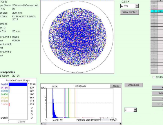
Before intensive cleaning, it is essential to assess existing surface contamination. Understanding the type, size distribution, and spatial arrangement of contaminants on the wafer surface optimizes cleaning chemistry and mechanical energy input.
3. Advanced Analytical Techniques for Contamination Assessment
3.1 Surface Particle Analysis
- Specialized particle counters utilize laser scattering or computer vision to count, size, and map surface debris.
- Light scattering intensity correlates with particle sizes as small as tens of nanometers and densities as low as 0.1 particles/cm².
- Calibration with standards ensures hardware reliability. Pre- and post-cleaning scans validate removal efficiency, driving process improvements.
3.2 Elemental Surface Analysis
- Surface-sensitive techniques identify elemental composition.
- X-ray Photoelectron Spectroscopy (XPS/ESCA): Analyzes surface chemical states by irradiating the wafer with X-rays and measuring emitted electrons.
- Glow Discharge Optical Emission Spectroscopy (GD-OES): Sputters ultra-thin surface layers sequentially while analyzing emitted spectra to determine depth-dependent elemental composition.
- Detection limits reach parts per million (ppm), guiding optimal cleaning chemistry selection.
3.3 Morphological Contamination Analysis
- Scanning Electron Microscopy (SEM): Captures high-resolution images to reveal contaminants’ shapes and aspect ratios, indicating adhesion mechanisms (chemical vs. mechanical).
- Atomic Force Microscopy (AFM): Maps nanoscale topography to quantify particle height and mechanical properties.
- Focused Ion Beam (FIB) Milling + Transmission Electron Microscopy (TEM): Provides internal views of buried contaminants.
4. Advanced Cleaning Methods
While solvent cleaning effectively removes organic contaminants, additional advanced techniques are required for inorganic particles, metallic residues, and ionic contaminants:
4.1 RCA Cleaning
- Developed by RCA Laboratories, this method employs a dual-bath process to remove polar contaminants.
- SC-1 (Standard Clean-1): Removes organic contaminants and particles using a mixture of NH₄OH, H₂O₂, and H₂O (e.g., 1:1:5 ratio at ~20°C). Forms a thin silicon dioxide layer.
- SC-2 (Standard Clean-2): Removes metallic impurities using HCl, H₂O₂, and H₂O (e.g., 1:1:6 ratio at ~80°C). Leaves a passivated surface.
- Balances cleanliness with surface protection.
4.2 Ozone Purification
- Immerses wafers in ozone-saturated deionized water (O₃/H₂O).
- Effectively oxidizes and removes organics without damaging the wafer, leaving a chemically passivated surface.
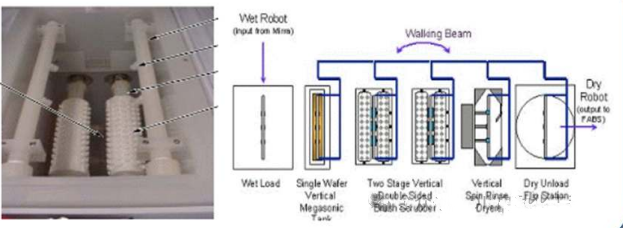
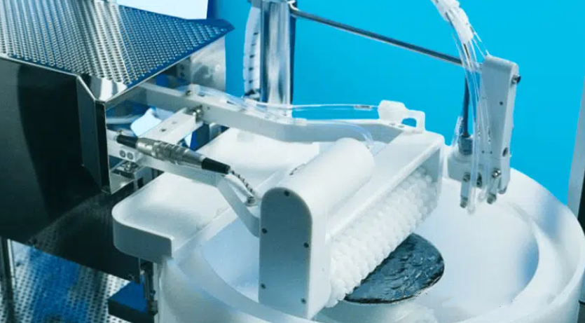
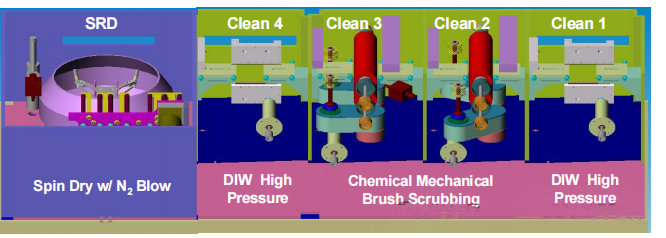
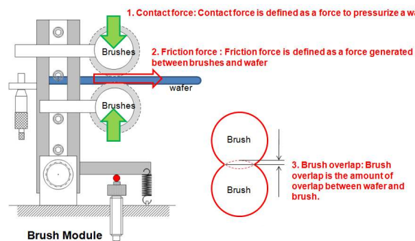
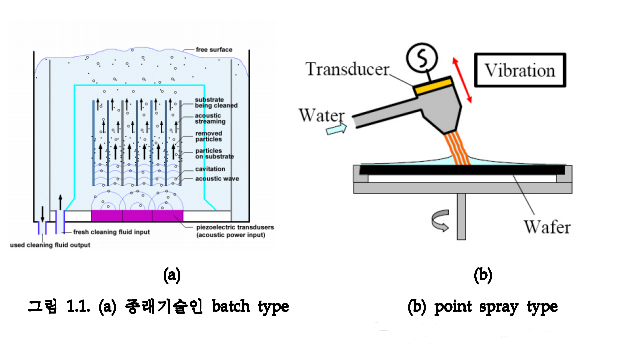
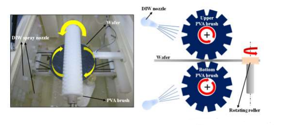
4.3 Megasonic Cleaning
- Utilizes high-frequency ultrasonic energy (typically 750–900 kHz) coupled with cleaning solutions.
- Generates cavitation bubbles that dislodge contaminants. Penetrates complex geometries while minimizing damage to delicate structures.
4.4 Cryogenic Cleaning
- Rapidly cools wafers to cryogenic temperatures, brittling contaminants.
- Subsequent rinsing or gentle brushing removes loosened particles. Prevents recontamination and diffusion into the surface.
- Fast, dry process with minimal chemical usage.
Conclusion:
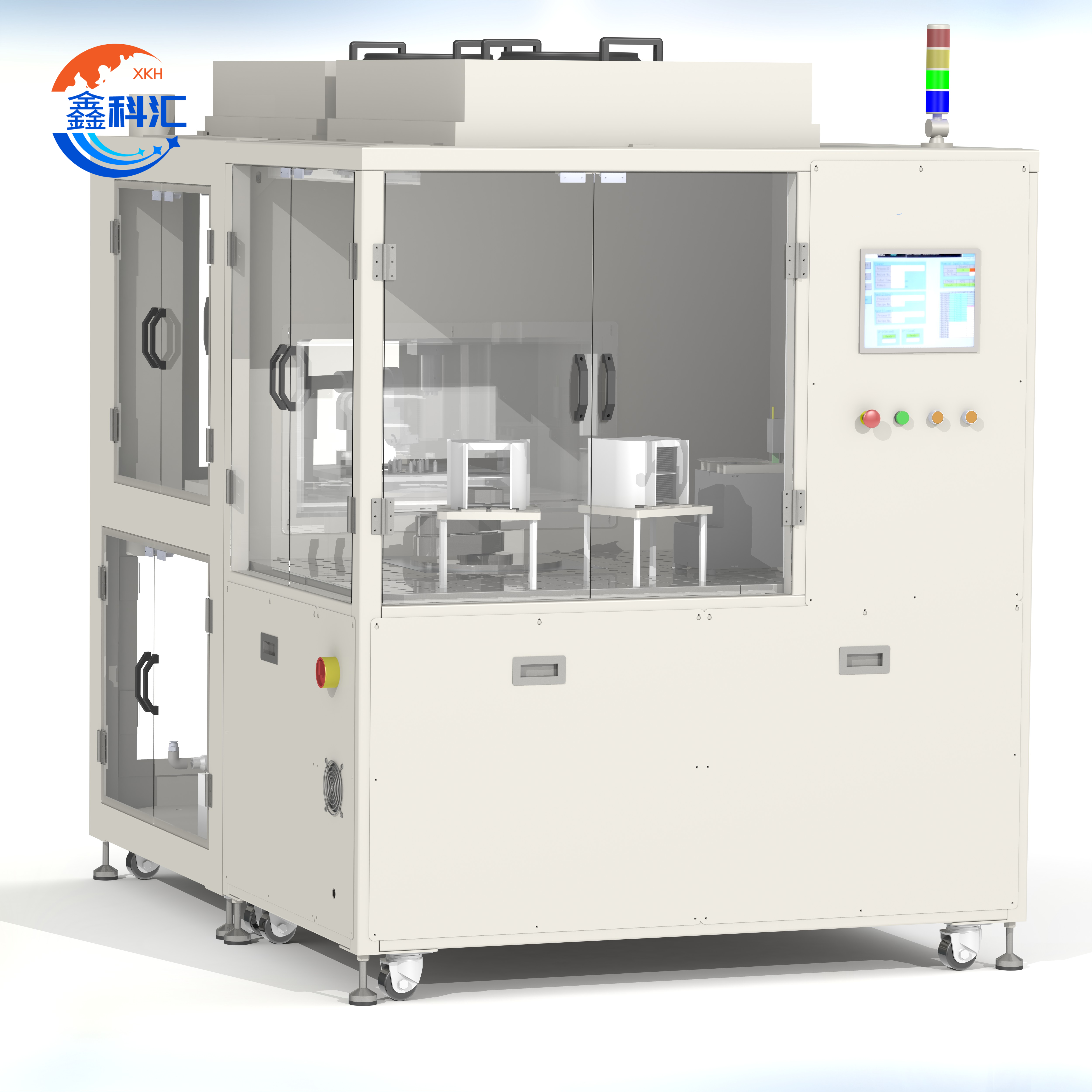
As a leading full-chain semiconductor solutions provider, XKH is driven by technological innovation and customer needs to deliver an end-to-end service ecosystem encompassing high-end equipment supply, wafer fabrication, and precision cleaning. We not only supply internationally recognized semiconductor equipment (e.g., lithography machines, etching systems) with tailored solutions but also pioneer proprietary technologies—including RCA cleaning, ozone purification, and megasonic cleaning—to ensure atomic-level cleanliness for wafer manufacturing, significantly enhancing client yield and production efficiency. Leveraging localized rapid-response teams and intelligent service networks, we provide comprehensive support ranging from equipment installation and process optimization to predictive maintenance, empowering clients to overcome technical challenges and advance toward higher precision and sustainable semiconductor development. Choose us for a dual-win synergy of technical expertise and commercial value.
Post time: Sep-02-2025