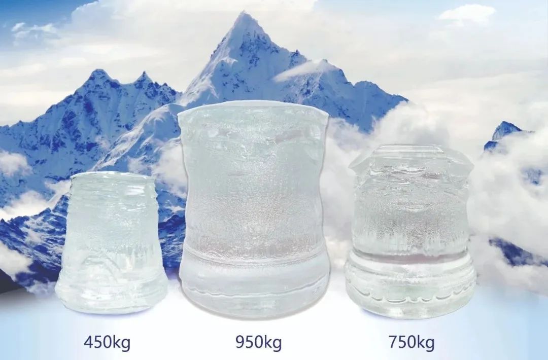
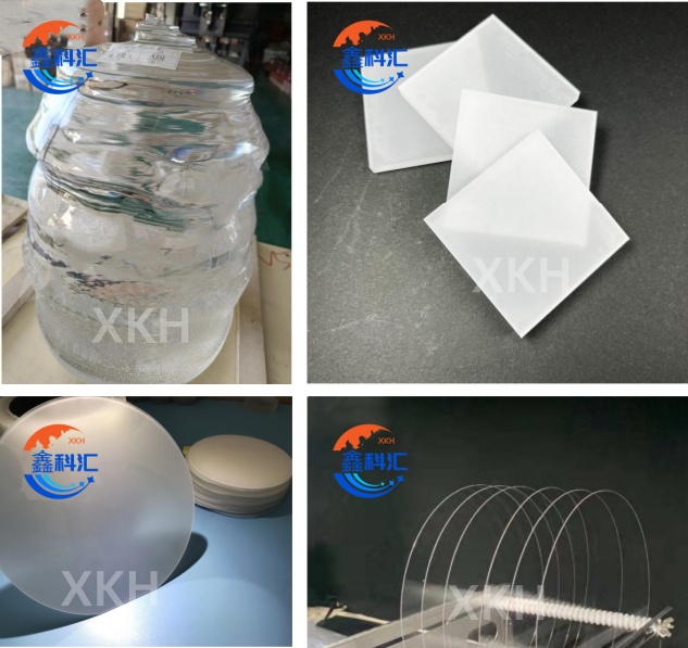
Sapphire crystals are grown from high-purity alumina powder with a purity of >99.995%, making them the largest demand area for high-purity alumina. They exhibit high strength, high hardness, and stable chemical properties, enabling them to operate in harsh environments such as high temperatures, corrosion, and impact. They are widely used in national defense, civilian technology, microelectronics, and other fields.
 From high-purity alumina powder to sapphire crystals
1. Key Applications of Sapphire
In the defense sector, sapphire crystals are primarily used for missile infrared windows. Modern warfare demands high precision in missiles, and the infrared optical window is a critical component to achieve this requirement. Considering that missiles experience intense aerodynamic heat and impact during high-speed flight, along with harsh combat environments, the radome must possess high strength, impact resistance, and the ability to withstand erosion from sand, rain, and other severe weather conditions. Sapphire crystals, with their excellent light transmission, superior mechanical properties, and stable chemical characteristics, have become an ideal material for missile infrared windows.
LED substrates represent the largest application of sapphire. LED lighting is considered the third revolution after fluorescent and energy-saving lamps. The principle of LEDs involves converting electrical energy into light energy. When current passes through a semiconductor, holes and electrons combine, releasing excess energy in the form of light, ultimately producing illumination. LED chip technology is based on epitaxial wafers, where gaseous materials are deposited layer by layer onto a substrate. The main substrate materials include silicon substrates, silicon carbide substrates, and sapphire substrates. Among these, sapphire substrates offer significant advantages over the other two, including device stability, mature preparation technology, non-absorption of visible light, good light transmittance, and moderate cost. Data shows that 80% of global LED companies use sapphire as their substrate material.
In addition to the aforementioned applications, sapphire crystals are also used in mobile phone screens, medical devices, jewelry decoration, and as window materials for various scientific detection instruments such as lenses and prisms.
2. Market Size and Prospects
Driven by policy support and the expanding application scenarios of LED chips, the demand for sapphire substrates and their market size are expected to achieve double-digit growth. By 2025, the shipment volume of sapphire substrates is projected to reach 103 million pieces (converted to 4-inch substrates), representing a 63% increase compared to 2021, with a compound annual growth rate (CAGR) of 13% from 2021 to 2025. The market size of sapphire substrates is expected to reach ¥8 billion by 2025, a 108% increase compared to 2021, with a CAGR of 20% from 2021 to 2025. As the “precursor” to substrates, the market size and growth trend of sapphire crystals are evident.
3. Preparation of Sapphire Crystals
Since 1891, when French chemist Verneuil A. invented the flame fusion method to produce artificial gem crystals for the first time, the study of artificial sapphire crystal growth has spanned over a century. During this period, advancements in science and technology have driven extensive research into sapphire growth techniques to meet industrial demands for higher crystal quality, improved utilization rates, and reduced production costs. Various new methods and technologies have emerged for growing sapphire crystals, such as the Czochralski method, Kyropoulos method, edge-defined film-fed growth (EFG) method, and heat exchange method (HEM).
3.1 Czochralski Method for Growing Sapphire Crystals
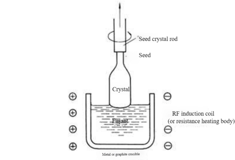
The Czochralski method, pioneered by Czochralski J. in 1918, is also known as the Czochralski technique (abbreviated as the Cz method). In 1964, Poladino A.E. and Rotter B.D. first applied this method to grow sapphire crystals. To date, it has produced a large number of high-quality sapphire crystals. The principle involves melting the raw material to form a melt, then dipping a single crystal seed into the melt surface. Due to the temperature difference at the solid-liquid interface, supercooling occurs, causing the melt to solidify on the seed surface and begin growing a single crystal with the same crystal structure as the seed. The seed is slowly pulled upward while rotating at a certain speed. As the seed is pulled, the melt gradually solidifies at the interface, forming a single crystal. This method, which involves pulling a crystal from the melt, is one of the common techniques for preparing high-quality single crystals.
The advantages of the Czochralski method include: (1) fast growth rate, enabling the production of high-quality single crystals in a short time; (2) crystals grow at the melt surface without contact with the crucible wall, effectively reducing internal stress and improving crystal quality. However, a major drawback of this method is the difficulty in growing large-diameter crystals, making it less suitable for producing large-sized crystals.
3.2 Kyropoulos Method for Growing Sapphire Crystals
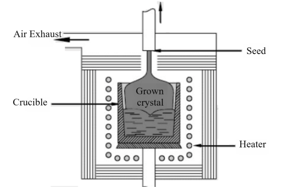
The Kyropoulos method, invented by Kyropoulos in 1926 (abbreviated as the KY method), shares similarities with the Czochralski method. It involves dipping a seed crystal into the melt surface and slowly pulling it upward to form a neck. Once the solidification rate at the melt-seed interface stabilizes, the seed is no longer pulled or rotated. Instead, the cooling rate is controlled to allow the single crystal to solidify gradually from the top downward, ultimately forming a single crystal.
The Kyropoulos process produces crystals with high quality, low defect density, large, and favorable cost-effectiveness.
3.3 Edge-Defined Film-Fed Growth (EFG) Method for Growing Sapphire Crystals
The EFG method is a shaped crystal growth technology. Its principle involves placing a high-melting-point melt into a mold. The melt is drawn to the top of the mold via capillary action, where it contacts the seed crystal. As the seed is pulled and the melt solidifies, a single crystal forms. The size and shape of the mold edge restrict the crystal dimensions. Consequently, this method has certain limitations and is primarily suitable for shaped sapphire crystals such as tubes and U-shaped profiles.
3.4 Heat Exchange Method (HEM) for Growing Sapphire Crystals
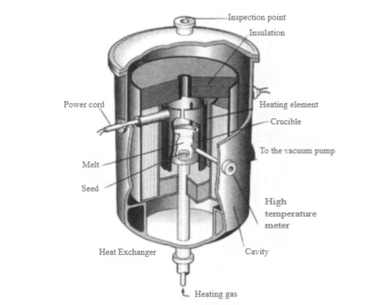
The heat exchange method for preparing large-sized sapphire crystals was invented by Fred Schmid and Dennis in 1967. The HEM system features excellent thermal insulation, independent control of the temperature gradient in the melt and crystal, and good controllability. It relatively easily produces sapphire crystals with low dislocation and large.
The advantages of the HEM method include the absence of movement in the crucible, crystal, and heater during growth, eliminating pulling actions such as those in the Kyropoulos and Czochralski methods. This reduces human interference and avoids crystal defects caused by mechanical motion. Additionally, the cooling rate can be controlled to minimize thermal stress and resulting crystal cracking and dislocation defects. This method enables the growth of large-sized crystals, is relatively easy to operate, and holds promising development prospects.
Leveraging deep expertise in sapphire crystal growth and precision processing, XKH provides end-to-end custom sapphire wafer solutions tailored to defense, LED, and optoelectronics applications. In addition to sapphire, we supply a full range of high-performance semiconductor materials including silicon carbide (SiC) wafers, silicon wafers, SiC ceramic components, and quartz products. We ensure exceptional quality, reliability, and technical support across all materials, helping customers achieve breakthrough performance in advanced industrial and research applications.
Post time: Aug-29-2025

