From the working principle of LEDs, it is evident that the epitaxial wafer material is the core component of an LED. In fact, key optoelectronic parameters such as wavelength, brightness, and forward voltage are largely determined by the epitaxial material. Epitaxial wafer technology and equipment are critical to the manufacturing process, with Metal-Organic Chemical Vapor Deposition (MOCVD) being the primary method for growing thin single-crystal layers of III-V, II-VI compounds, and their alloys. Below are some future trends in LED epitaxial wafer technology.
1. Improvement of Two-Step Growth Process
Currently, commercial production employs a two-step growth process, but the number of substrates that can be loaded at once is limited. While 6-wafer systems are mature, machines handling around 20 wafers are still under development. Increasing the number of wafers often leads to insufficient uniformity in epitaxial layers. Future developments will focus on two directions:
- Developing technologies that allow loading more substrates in a single reaction chamber, making them more suitable for large-scale production and cost reduction.
- Advancing highly automated, repeatable single-wafer equipment.
2. Hydride Vapor Phase Epitaxy (HVPE) Technology
This technology enables rapid growth of thick films with low dislocation density, which can serve as substrates for homoepitaxial growth using other methods. Additionally, GaN films separated from the substrate may become alternatives to bulk GaN single-crystal chips. However, HVPE has drawbacks, such as difficulty in precise thickness control and corrosive reaction gases that hinder further improvement in GaN material purity.
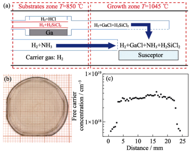
Si-doped HVPE-GaN
(a) Structure of Si-doped HVPE-GaN reactor; (b) Image of 800 μm- thick Si-doped HVPE-GaN;
(c) Distribution of free carrier concentration along the diameter of Si-doped HVPE-GaN
3. Selective Epitaxial Growth or Lateral Epitaxial Growth Technology
This technique can further reduce dislocation density and improve the crystal quality of GaN epitaxial layers. The process involves:
- Depositing a GaN layer on a suitable substrate (sapphire or SiC).
- Depositing a polycrystalline SiO₂ mask layer on top.
- Using photolithography and etching to create GaN windows and SiO₂ mask strips.During subsequent growth, GaN first grows vertically in the windows and then laterally over the SiO₂ strips.
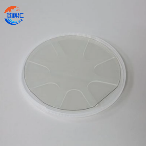
XKH’s GaN-on-Sapphire wafer
4. Pendeo-Epitaxy Technology
This method significantly reduces lattice defects caused by lattice and thermal mismatch between the substrate and epitaxial layer, further enhancing GaN crystal quality. The steps include:
- Growing a GaN epitaxial layer on a suitable substrate (6H-SiC or Si) using a two-step process.
- Performing selective etching of the epitaxial layer down to the substrate, creating alternating pillar (GaN/buffer/substrate) and trench structures.
- Growing additional GaN layers, which extend laterally from the sidewalls of the original GaN pillars, suspended over the trenches.Since no mask is used, this avoids contact between GaN and mask materials.
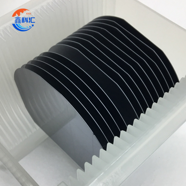
XKH’s GaN-on-Silicon wafer
5. Development of Short-Wavelength UV LED Epitaxial Materials
This lays a solid foundation for UV-excited phosphor-based white LEDs. Many high-efficiency phosphors can be excited by UV light, offering higher luminous efficiency than the current YAG:Ce system, thereby advancing white LED performance.
6. Multi-Quantum Well (MQW) Chip Technology
In MQW structures, different impurities are doped during the growth of the light-emitting layer to create varying quantum wells. The recombination of photons emitted from these wells produces white light directly. This method improves luminous efficiency, reduces costs, and simplifies packaging and circuit control, though it presents greater technical challenges.
7. Development of “Photon Recycling” Technology
In January 1999, Japan’s Sumitomo developed a white LED using ZnSe material. The technology involves growing a CdZnSe thin film on a ZnSe single-crystal substrate. When electrified, the film emits blue light, which interacts with the ZnSe substrate to produce complementary yellow light, resulting in white light. Similarly, Boston University’s Photonics Research Center stacked an AlInGaP semiconductor compound on a blue GaN-LED to generate white light.
8. LED Epitaxial Wafer Process Flow
① Epitaxial Wafer Fabrication:
Substrate → Structural design → Buffer layer growth → N-type GaN layer growth → MQW light-emitting layer growth → P-type GaN layer growth → Annealing → Testing (photoluminescence, X-ray) → Epitaxial wafer
② Chip Fabrication:
Epitaxial wafer → Mask design and fabrication → Photolithography → Ion etching → N-type electrode (deposition, annealing, etching) → P-type electrode (deposition, annealing, etching) → Dicing → Chip inspection and grading.
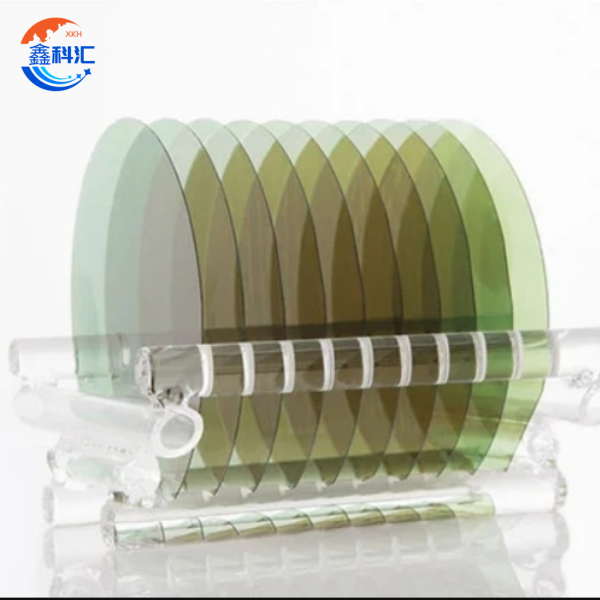
ZMSH’s GaN-on-SiC wafer
Post time: Jul-25-2025