Although both silicon and glass wafers share the common goal of being “cleaned,” the challenges and failure modes they face during cleaning are vastly different. This discrepancy arises from the inherent material properties and specification requirements of silicon and glass, as well as the distinct “philosophy” of cleaning driven by their final applications.
First, let’s clarify: What exactly are we cleaning? What contaminants are involved?
Contaminants can be classified into four categories:
-
Particle Contaminants
-
Dust, metal particles, organic particles, abrasive particles (from CMP process), etc.
-
These contaminants can cause pattern defects, such as shorts or open circuits.
-
-
Organic Contaminants
-
Includes photoresist residues, resin additives, human skin oils, solvent residues, etc.
-
Organic contaminants can form masks that hinder etching or ion implantation and reduce adhesion of other thin films.
-
-
Metal Ion Contaminants
-
Iron, copper, sodium, potassium, calcium, etc., which primarily come from equipment, chemicals, and human contact.
-
In semiconductors, metal ions are “killer” contaminants, introducing energy levels in the forbidden band, which increase leakage current, shorten carrier lifetime, and severely damage electrical properties. In glass, they may affect the quality and adhesion of subsequent thin films.
-
-
Native Oxide Layer
-
For silicon wafers: A thin layer of silicon dioxide (Native Oxide) naturally forms on the surface in the air. The thickness and uniformity of this oxide layer are difficult to control, and it must be completely removed during the fabrication of key structures such as gate oxides.
-
For glass wafers: Glass itself is a silica network structure, so there is no issue of “removing a native oxide layer.” However, the surface may have been modified due to contamination, and this layer needs to be removed.
-

I. Core Goals: The Divergence Between Electrical Performance and Physical Perfection
-
Silicon Wafers
-
The core goal of cleaning is to ensure electrical performance. Specifications typically include strict particle counts and sizes (e.g., particles ≥0.1μm must be effectively removed), metal ion concentrations (e.g., Fe, Cu must be controlled to ≤10¹⁰ atoms/cm² or lower), and organic residue levels. Even microscopic contamination can lead to circuit shorts, leakage currents, or failure of gate oxide integrity.
-
-
Glass Wafers
-
As substrates, the core requirements are physical perfection and chemical stability. Specifications focus on macro-level aspects such as the absence of scratches, non-removable stains, and the maintenance of the original surface roughness and geometry. The cleaning goal is primarily to ensure visual cleanliness and good adhesion for subsequent processes such as coating.
-
II. Material Nature: The Fundamental Difference Between Crystalline and Amorphous
-
Silicon
-
Silicon is a crystalline material, and its surface naturally grows a non-uniform silicon dioxide (SiO₂) oxide layer. This oxide layer poses a risk to electrical performance and must be thoroughly and uniformly removed.
-
-
Glass
-
Glass is an amorphous silica network. Its bulk material is similar in composition to the silicon oxide layer of silicon, which means it can be quickly etched by hydrofluoric acid (HF) and is also susceptible to strong alkali erosion, leading to an increase in surface roughness or deformation. This fundamental difference dictates that silicon wafer cleaning can tolerate light, controlled etching to remove contaminants, while glass wafer cleaning must be performed with extreme care to avoid damaging the base material.
-
| Cleaning Item | Silicon Wafer Cleaning | Glass Wafer Cleaning |
|---|---|---|
| Cleaning Goal | Includes its own native oxide layer | Select cleaning method: Remove contaminants while protecting base material |
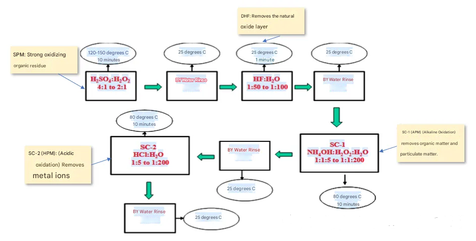
| Standard RCA Cleaning | - SPM (H₂SO₄/H₂O₂): Removes organic/photoresist residues | Main Cleaning Flow: |
| - SC1 (NH₄OH/H₂O₂/H₂O): Removes surface particles | Weak Alkaline Cleaning Agent: Contains active surface agents to remove organic contaminants and particles | |
| - DHF (Hydrofluoric acid): Removes natural oxide layer and other contaminants | Strong Alkaline or Middle Alkaline Cleaning Agent: Used to remove metallic or non-volatile contaminants | |
| - SC2 (HCl/H₂O₂/H₂O): Removes metal contaminants | Avoid HF throughout | |
| Key Chemicals | Strong acids, strong alkalis, oxidizing solvents | Weak alkaline cleaning agent, specifically formulated for mild contamination removal |
| Physical Aids | Deionized water (for high-purity rinsing) | Ultrasonic, megasonic washing |
| Drying Technology | Megasonic, IPA vapor drying | Gentle drying: Slow lift, IPA vapor drying |
III. Comparison of Cleaning Solutions
Based on the aforementioned goals and material characteristics, the cleaning solutions for silicon and glass wafers differ:
| Silicon Wafer Cleaning | Glass Wafer Cleaning | |
|---|---|---|
| Cleaning objective | Thorough removal, including the wafer’s native oxide layer. | Selective removal: eliminate contaminants while protecting the substrate. |
| Typical process | Standard RCA clean: • SPM (H₂SO₄/H₂O₂): removes heavy organics/photoresist • SC1 (NH₄OH/H₂O₂/H₂O): alkaline particle removal • DHF (dilute HF): removes native oxide layer and metals • SC2 (HCl/H₂O₂/H₂O): removes metal ions | Characteristic cleaning flow: • Mild-alkaline cleaner with surfactants to remove organics and particles • Acidic or neutral cleaner for removing metal ions and other specific contaminants • Avoid HF throughout the process |
| Key chemicals | Strong acids, strong oxidizers, alkaline solutions | Mild-alkaline cleaners; specialized neutral or slightly acidic cleaners |
| Physical assist | Megasonic (high-efficiency, gentle particle removal) | Ultrasonic, megasonic |
| Drying | Marangoni drying; IPA vapor drying | Slow-pull drying; IPA vapor drying |
-
Glass Wafer Cleaning Process
-
Currently, most glass processing plants use cleaning procedures based on the material characteristics of glass, relying primarily on weak alkaline cleaning agents.
-
Cleaning Agent Characteristics: These specialized cleaning agents are typically weakly alkaline, with a pH around 8-9. They usually contain surfactants (e.g., alkyl polyoxyethylene ether), metal chelating agents (e.g., HEDP), and organic cleaning aids, designed to emulsify and decompose organic contaminants such as oils and fingerprints, while being minimally corrosive to the glass matrix.
-
Process Flow: The typical cleaning process involves using a specific concentration of weak alkaline cleaning agents at temperatures ranging from room temperature to 60°C, combined with ultrasonic cleaning. After cleaning, the wafers undergo multiple rinsing steps with pure water and gentle drying (e.g., slow lifting or IPA vapor drying). This process effectively meets the glass wafer requirements for visual cleanliness and general cleanliness.
-
-
Silicon Wafer Cleaning Process
-
For semiconductor processing, silicon wafers typically undergo standard RCA cleaning, which is a highly effective cleaning method capable of systematically addressing all types of contaminants, ensuring that the electrical performance requirements for semiconductor devices are met.
-
IV. When Glass Meets Higher “Cleanliness” Standards
When glass wafers are used in applications requiring stringent particle counts and metal ion levels (e.g., as substrates in semiconductor processes or for excellent thin film deposition surfaces), the intrinsic cleaning process may no longer be sufficient. In this case, semiconductor cleaning principles can be applied, introducing a modified RCA cleaning strategy.
The core of this strategy is to dilute and optimize the standard RCA process parameters to accommodate the sensitive nature of glass:
-
Organic Contaminant Removal: SPM solutions or milder ozone water can be used to decompose organic contaminants through strong oxidation.
-
Particle Removal: Highly diluted SC1 solution is employed at lower temperatures and shorter treatment times to utilize its electrostatic repulsion and micro-etching effects to remove particles, while minimizing corrosion on the glass.
-
Metal Ion Removal: A diluted SC2 solution or simple dilute hydrochloric acid/dilute nitric acid solutions are used to remove metal contaminants via chelation.
-
Strict Prohibitions: DHF (di-ammonium fluoride) must be absolutely avoided to prevent corrosion of the glass substrate.
In the entire modified process, combining megasonic technology significantly enhances the removal efficiency of nano-sized particles and is gentler on the surface.
Conclusion
The cleaning processes for silicon and glass wafers are the inevitable result of reverse engineering based on their final application requirements, material properties, and physical and chemical characteristics. Silicon wafer cleaning seeks “atomic-level cleanliness” for electrical performance, while glass wafer cleaning focuses on achieving “perfect, undamaged” physical surfaces. As glass wafers are increasingly used in semiconductor applications, their cleaning processes will inevitably evolve beyond traditional weak alkaline cleaning, developing more refined, customized solutions like the modified RCA process to meet higher cleanliness standards.
Post time: Oct-29-2025