Semiconductors serve as the cornerstone of the information age, with each material iteration redefining the boundaries of human technology. From first-generation silicon-based semiconductors to today’s fourth-generation ultra-wide bandgap materials, every evolutionary leap has driven transformative advancements in communications, energy, and computing. By analyzing the characteristics and generational transition logic of existing semiconductor materials, we can predict potential directions for fifth-generation semiconductors while exploring China’s strategic pathways in this competitive arena.
I. Characteristics and Evolutionary Logic of Four Semiconductor Generations
First-Generation Semiconductors: The Silicon-Germanium Foundation Era
Characteristics: Elemental semiconductors like silicon (Si) and germanium (Ge) offer cost-effectiveness and mature manufacturing processes, yet suffer from narrow bandgaps (Si: 1.12 eV; Ge: 0.67 eV), limiting voltage tolerance and high-frequency performance.
Applications: Integrated circuits, solar cells, low-voltage/low-frequency devices.
Transition Driver: Growing demand for high-frequency/high-temperature performance in optoelectronics outpaced silicon’s capabilities.
Second-Generation Semiconductors: The III-V Compound Revolution
Characteristics: III-V compounds like gallium arsenide (GaAs) and indium phosphide (InP) feature wider bandgaps (GaAs: 1.42 eV) and high electron mobility for RF and photonic applications.
Applications: 5G RF devices, laser diodes, satellite communications.
Challenges: Material scarcity (indium abundance: 0.001%), toxic elements (arsenic), and high production costs.
Transition Driver: Energy/power applications demanded materials with higher breakdown voltages.
Third-Generation Semiconductors: Wide Bandgap Energy Revolution
Characteristics: Silicon carbide (SiC) and gallium nitride (GaN) deliver bandgaps >3eV (SiC:3.2eV; GaN:3.4eV), with superior thermal conductivity and high-frequency characteristics.
Applications: EV powertrains, PV inverters, 5G infrastructure.
Advantages: 50%+ energy savings and 70% size reduction versus silicon.
Transition Driver: AI/quantum computing requires materials with extreme performance metrics.
Fourth-Generation Semiconductors: Ultra-Wide Bandgap Frontier
Characteristics: Gallium oxide (Ga₂O₃) and diamond (C) achieve bandgaps up to 4.8eV, combining ultra-low on-resistance with kV-class voltage tolerance.
Applications: Ultra-high-voltage ICs, deep-UV detectors, quantum communication.
Breakthroughs: Ga₂O₃ devices withstand >8kV, tripling SiC’s efficiency.
Evolutionary Logic: Quantum-scale performance leaps are needed to overcome physical limits.
I. Fifth-Generation Semiconductor Trends: Quantum Materials & 2D Architectures
Potential development vectors include:
1. Topological Insulators: Surface conduction with bulk insulation enables zero-loss electronics.
2. 2D Materials: Graphene/MoS₂ offer THz-frequency response and flexible electronics compatibility.
3. Quantum Dots & Photonic Crystals: Bandgap engineering enables optoelectronic-thermal integration.
4. Bio-Semiconductors: DNA/protein-based self-assembling materials bridge biology and electronics.
5. Key Drivers: AI, brain-computer interfaces, and room-temperature superconductivity demands.
II. China’s Semiconductor Opportunities: From Follower to Leader
1. Technology Breakthroughs
• 3rd-Gen: Mass production of 8-inch SiC substrates; automotive-grade SiC MOSFETs in BYD vehicles
• 4th-Gen: 8-inch Ga₂O₃ epitaxy breakthroughs by XUPT and CETC46
2. Policy Support
• 14th Five-Year Plan prioritizes 3rd-gen semiconductors
• Provincial hundred-billion-yuan industrial funds established
• Milestones 6-8 inch GaN devices and Ga₂O₃ transistors listed among top-10 tech advancements in 2024
III. Challenges and Strategic Solutions
1. Technical Bottlenecks
• Crystal Growth: Low yield for large-diameter boules (e.g., Ga₂O₃ cracking)
• Reliability Standards: Lack of established protocols for high-power/high-frequency aging tests
2. Supply Chain Gaps
• Equipment: <20% domestic content for SiC crystal growers
• Adoption: Downstream preference for imported components
3. Strategic Pathways
• Industry-Academia Collaboration: Modeled after the “Third-Gen Semiconductor Alliance”
• Niche Focus: Prioritize quantum communications/new energy markets
• Talent Development: Establish “Chip Science & Engineering” academic programs
From silicon to Ga₂O₃, semiconductor evolution chronicles humanity’s triumph over physical limits. China’s opportunity lies in mastering fourth-gen materials while pioneering fifth-gen innovations. As Academician Yang Deren noted: “True innovation requires forging untraveled paths.” The synergy of policy, capital, and technology will determine China’s semiconductor destiny.
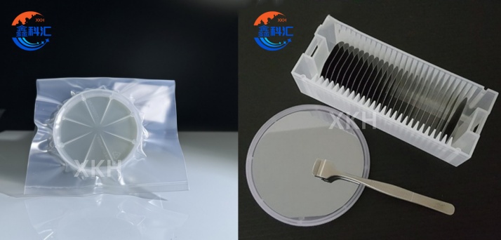
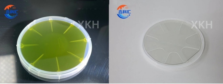
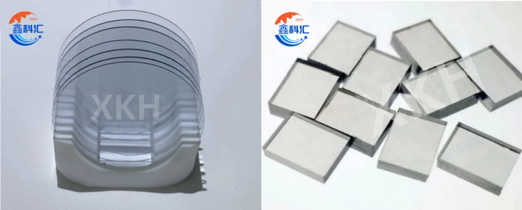
XKH has emerged as a vertically integrated solutions provider specializing in advanced semiconductor materials across multiple technology generations. With core competencies spanning crystal growth, precision processing, and functional coating technologies, XKH delivers high-performance substrates and epitaxial wafers for cutting-edge applications in power electronics, RF communications, and optoelectronic systems. Our manufacturing ecosystem encompasses proprietary processes for producing 4-8 inch silicon carbide and gallium nitride wafers with industry-leading defect control, while maintaining active R&D programs in emerging ultra-wide bandgap materials including gallium oxide and diamond semiconductors. Through strategic collaborations with leading research institutions and equipment manufacturers, XKH has developed a flexible production platform capable of supporting both high-volume manufacturing of standardized products and specialized development of customized material solutions. XKH’s technical expertise focuses on addressing critical industry challenges such as improving wafer uniformity for power devices, enhancing thermal management in RF applications, and developing novel heterostructures for next-generation photonic devices. By combining advanced material science with precision engineering capabilities, XKH enables customers to overcome performance limitations in high-frequency, high-power, and extreme environment applications while supporting the domestic semiconductor industry’s transition toward greater supply chain independence.
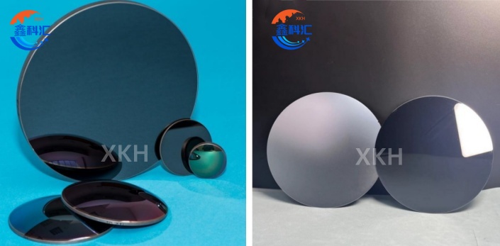
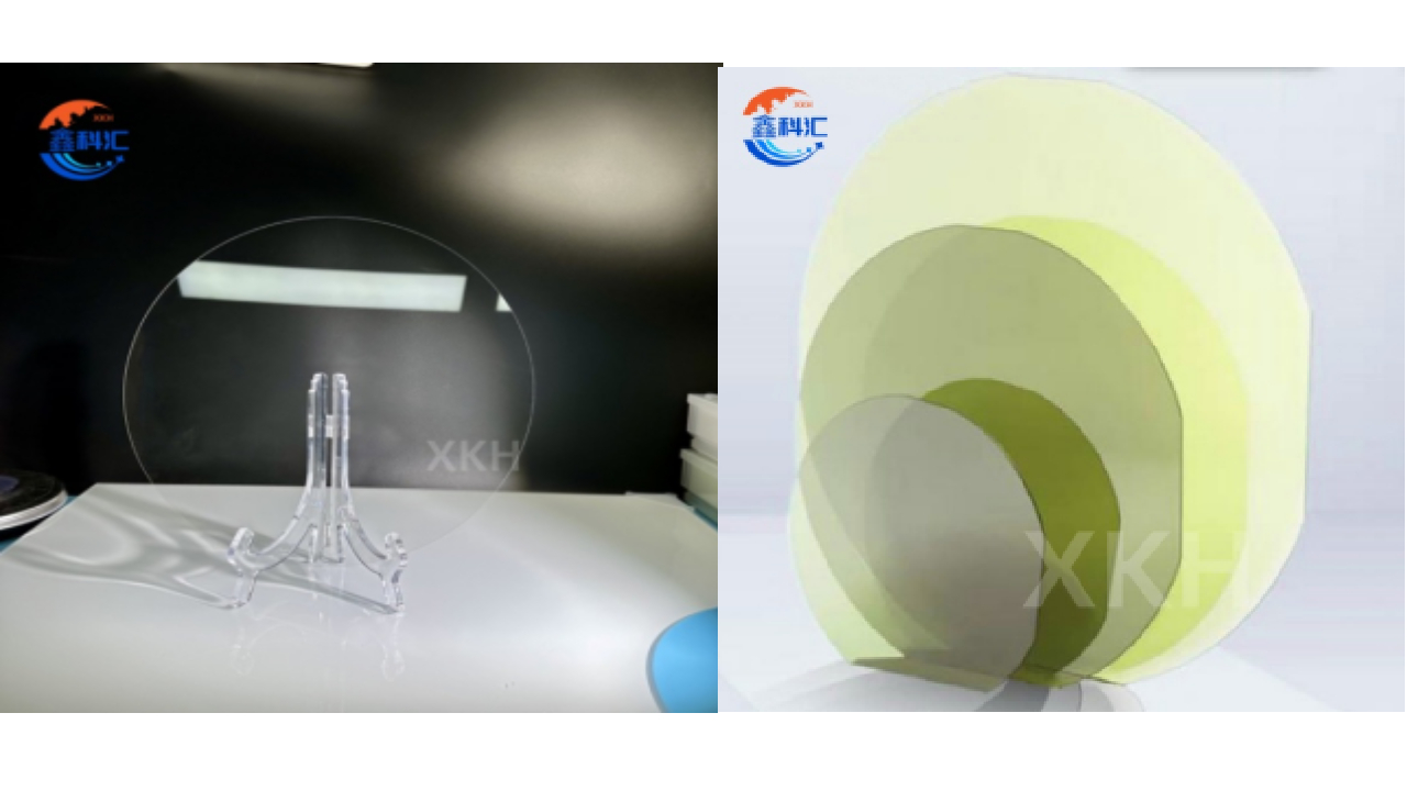
The following are XKH’s 12inchsapphire wafer & 12inch SiC substrate:
Post time: Jun-06-2025