Introduction
Inspired by the success of electronic integrated circuits (EICs), the field of photonic integrated circuits (PICs) has been evolving since its inception in 1969. However, unlike EICs, the development of a universal platform capable of supporting diverse photonic applications remains a major challenge. This article explores the emerging Lithium Niobate on Insulator (LNOI) technology, which has rapidly become a promising solution for next-generation PICs.
The Rise of LNOI Technology
Lithium niobate (LN) has long been recognized as a key material for photonic applications. However, only with the advent of thin-film LNOI and advanced fabrication techniques has its full potential been unlocked. Researchers have successfully demonstrated ultra-low-loss ridge waveguides and ultra-high-Q microresonators on LNOI platforms [1], marking a significant leap in integrated photonics.
Key Advantages of LNOI Technology
- Ultra-low optical loss (as low as 0.01 dB/cm)
- High-quality nanophotonic structures
- Support for diverse nonlinear optical processes
- Integrated electro-optic (EO) tunability
Nonlinear Optical Processes on LNOI
High-performance nanophotonic structures fabricated on the LNOI platform enable the realization of key nonlinear optical processes with remarkable efficiency and minimal pump power. Demonstrated processes include:
- Second Harmonic Generation (SHG)
- Sum Frequency Generation (SFG)
- Difference Frequency Generation (DFG)
- Parametric Down-Conversion (PDC)
- Four-Wave Mixing (FWM)
Various phase-matching schemes have been implemented to optimize these processes, establishing LNOI as a highly versatile nonlinear optical platform.
Electro-Optically Tunable Integrated Devices
LNOI technology has also enabled the development of a wide range of active and passive tunable photonic devices, such as:
- High-speed optical modulators
- Reconfigurable multifunctional PICs
- Tunable frequency combs
- Micro-optomechanical springs
These devices leverage the intrinsic EO properties of lithium niobate to achieve precise, high-speed control of light signals.
Practical Applications of LNOI Photonics
LNOI-based PICs are now being adopted in a growing number of practical applications, including:
- Microwave-to-optical converters
- Optical sensors
- On-chip spectrometers
- Optical frequency combs
- Advanced telecommunication systems
These applications demonstrate the potential of LNOI to match the performance of bulk-optic components, while offering scalable, energy-efficient solutions through photolithographic fabrication.
Current Challenges and Future Directions
Despite its promising progress, LNOI technology faces several technical hurdles:
a) Further Reducing Optical Loss
Current waveguide loss (0.01 dB/cm) is still an order of magnitude higher than the material absorption limit. Advances in ion-slicing techniques and nanofabrication are needed to reduce surface roughness and absorption-related defects.
b) Improved Waveguide Geometry Control
Enabling sub-700 nm waveguides and sub-2 μm coupling gaps without sacrificing repeatability or increasing propagation loss is crucial for higher integration density.
c) Enhancing Coupling Efficiency
While tapered fibers and mode converters help achieve high coupling efficiency, anti-reflection coatings can further mitigate air-material interface reflections.
d) Development of Low-Loss Polarization Components
Polarization-insensitive photonic devices on LNOI are essential, requiring components that match the performance of free-space polarizers.
e) Integration of Control Electronics
Effectively integrating large-scale control electronics without degrading optical performance is a key research direction.
f) Advanced Phase Matching and Dispersion Engineering
Reliable domain patterning at sub-micron resolution is vital for nonlinear optics but remains an immature technology on the LNOI platform.
g) Compensation for Fabrication Defects
Techniques to mitigate phase shifts caused by environmental changes or fabrication variances are essential for real-world deployment.
h) Efficient Multi-Chip Coupling
Addressing efficient coupling between multiple LNOI chips is necessary to scale beyond single-wafer integration limits.
Monolithic Integration of Active and Passive Components
A core challenge for LNOI PICs is the cost-effective monolithic integration of active and passive components such as:
- Lasers
- Detectors
- Nonlinear wavelength converters
- Modulators
- Multiplexers/Demultiplexers
Current strategies include:
a) Ion Doping of LNOI:
Selective doping of active ions into designated regions can lead to on-chip light sources.
b) Bonding and Heterogeneous Integration:
Bonding pre-fabricated passive LNOI PICs with doped LNOI layers or III-V lasers provides an alternative path.
c) Hybrid Active/Passive LNOI Wafer Fabrication:
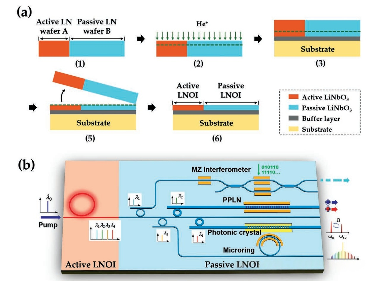
An innovative approach involves bonding doped and undoped LN wafers before ion slicing, resulting in LNOI wafers with both active and passive regions.
Figure 1 illustrates the concept of hybrid integrated active/passive PICs, where a single lithographic process enables seamless alignment and integration of both types of components.
Integration of Photodetectors
Integrating photodetectors into LNOI-based PICs is another crucial step toward fully functional systems. Two primary approaches are under investigation:
a) Heterogeneous Integration:
Semiconductor nanostructures can be transiently coupled to LNOI waveguides. However, improvements in detection efficiency and scalability are still required.
b) Nonlinear Wavelength Conversion:
LN’s nonlinear properties allow frequency conversion within waveguides, enabling the use of standard silicon photodetectors irrespective of operating wavelength.
Conclusion
The rapid advancement of LNOI technology brings the industry closer to a universal PIC platform capable of serving a broad range of applications. By addressing existing challenges and pushing forward innovations in monolithic and detector integration, LNOI-based PICs have the potential to revolutionize fields like telecommunications, quantum information, and sensing.
LNOI holds the promise of fulfilling the long-standing vision of scalable PICs, matching the success and impact of EICs. Continued R&D efforts—such as those from the Nanjing Photonics Process Platform and XiaoyaoTech Design Platform—will be pivotal in shaping the future of integrated photonics and unlocking new possibilities across technology domains.
Post time: Jul-18-2025